



Introduction
As many of you know, even if you’re not in the financial side of technical companies, NVIDIA published two numbers twelve hours apart this week. On Monday its engineers were at Hot Chips and they described a rack of 256 chips that holds 128 gibibytes of SRAM.
On Wednesday its CFO reported that the company has committed 279 billion dollars, primarily to buying DRAM: those are not separate stories. They are the same thing said twice, once by the engineering organisation and once by finance, and what connects them is a quantity that the standard formula for it gets wrong.
Everyone who deals with inference hardware knows the critical batch: the point where a decode step stops being memory bound and starts being compute bound, B* equals peak arithmetic times bytes per element over twice the memory bandwidth. On a Rubin package that is 398, whereas on the LPX rack it is 3.94. Those are the numbers I expected to build this piece on.
They describe a machine serving no context at all. The formula is derived from a decode step that reads only weights, and once you put the KV cache back into it the expression acquires a pole.
After a certain context length the denominator goes negative and no batch size makes the machine compute bound, because each additional sequence adds more memory traffic than amortisable arithmetic.
For Gemma 4 31B, the model NVIDIA benchmarked, a Rubin package reaches that point at 84 tokens. The LPX rack holds out to roughly 68,000. That precise gap, and not the 101 times in the spec sheets, is what NVIDIA spent 20 billion dollars to buy.
What follows is the derivation, the money behind it, and the places where I got it wrong first.
The short version
I want to introduce this section in this research post, so that you are able to take the core concepts and principles in the short form. I do really think that it will help, let me know if that’s the correct approach.
The critical batch formula in common use drops the KV term. Restored, it has a pole at the saturation context: 84 tokens on Rubin, 68,000 on the LPX rack, a ratio of 811 rather than 101.
Above saturation, raising batch buys capacity utilisation, not arithmetic utilisation. Throughput ceilings at memory bandwidth over cache bytes per sequence. For this model on an NVL72 that is about 143,000 tokens per second and no scheduler setting beats it.
At 100K of context the NVL72 makes 13 times the rack tokens. The LPX makes each user’s tokens arrive 45 times faster. That is the entire trade, measured at one context length.
The LPX is a latency product, not a bandwidth product. It runs 279 times below its own bandwidth roofline, and streaming plus arithmetic account for 0.43 percent of a token’s time budget.
SRAM is 1.4 to 6.4 times dearer per byte than HBM4 and 642 to 2,924 times cheaper per byte per second. Every design decision in the rack follows from that one ratio.
NVIDIA’s 279 billion dollar commitment, read against its own revenue guide, implies 28.2 dollars per gigabyte of HBM4, which lands within 11 percent of the price Korean and Taiwanese analysts publish. Two methods sharing no inputs.
The ledger
Let’s start with the disclosure, because it is unambiguous and it is filed directly with the SEC. NVIDIA reported revenue of 96,221 million dollars for the quarter ended 26 July 2026, of which 89,023 million was the Data Center section.
Gross margin was 75.0 percent on both a GAAP and a non-GAAP basis. Cost of revenue was precisely at 24,079 million.
Three things in the same document deserve more attention than this short description.
The first one is the commitment table. In the CFO commentary, Colette Kress wrote that supply commitments rose from 119 billion dollars a quarter ago to 279 billion, and attributed the increase to the procurement of memory.
The table below breaks it out by fiscal year: 92 billion for the remainder of FY2027, 87 for FY2028, 88 for FY2029, then 6, then 5, then 1.
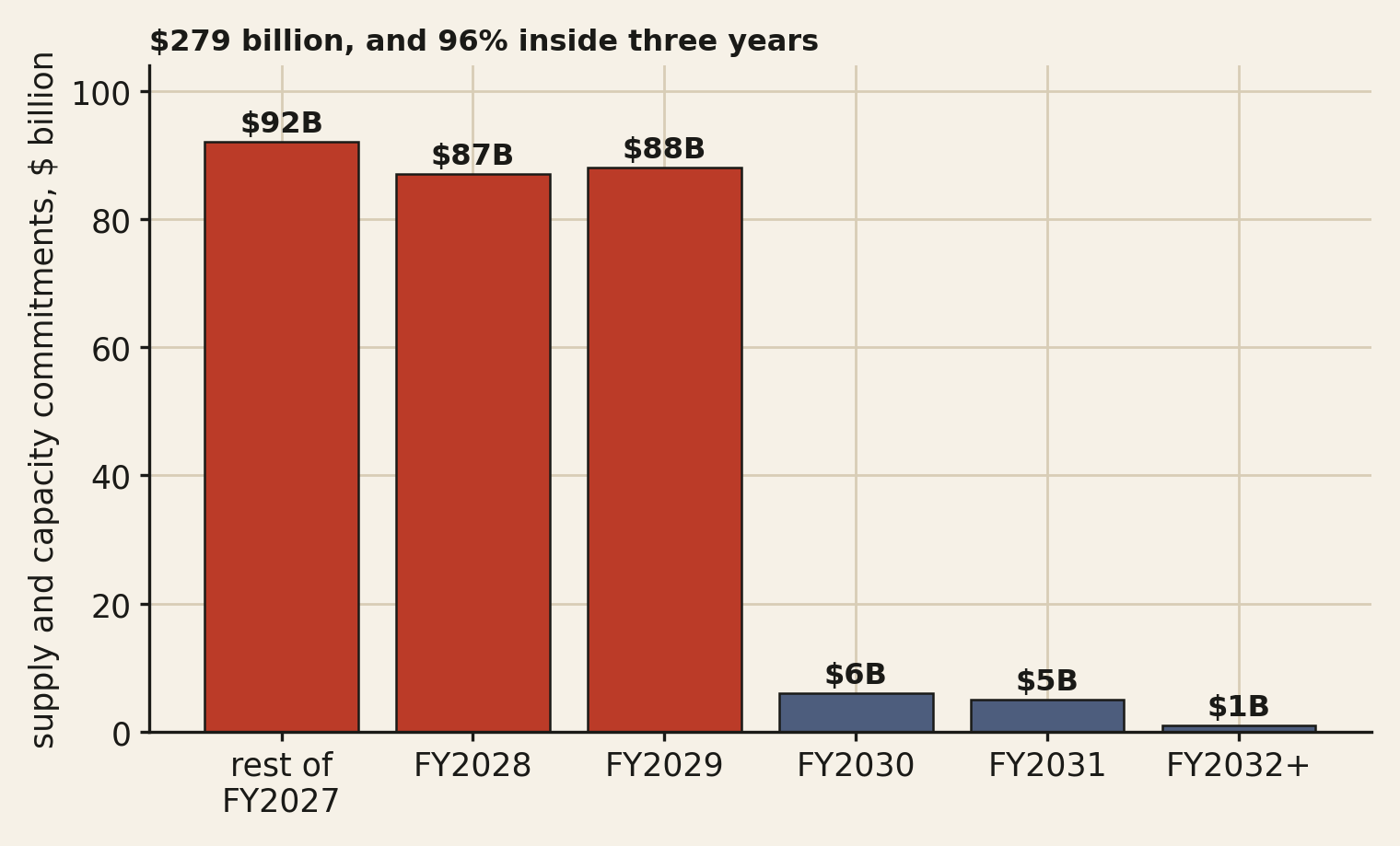
Ninety six percent of that money, 267 billion of the 279, lands inside three fiscal years. This isn’t a long-dated strategic reserve: it is a three year buy with a cliff at the end of it, which is what a purchase schedule looks like when you are securing a component whose supply is allocated rather than traded.
The second one is the guide, and it runs way further than the headline. NVIDIA guided Q3 revenue to 108 billion dollars and gross margin to 74.0 percent, a hundred basis points below the quarter it just reported. On the call Kress said that margin falls to 71 or 72 percent by the January quarter before recovering to 72 or 73 next year.
That is a three hundred to four hundred basis point trough, not a one hundred point wobble, and it is scheduled. On 108 billion, a hundred basis points is 1,080 million dollars of additional cost of revenue in a single quarter.
If memory is roughly 30 to 40 percent of accelerator manufacturing cost, which is the range the trade estimates converge on and which is consistent with the roughly 3,250 dollars of HBM3e against 850 dollars of logic die in a B200, then the entire memory bill in that quarter is somewhere between 8.4 and 11.2 billion dollars. The guide-down is about eleven percent of it.
The third is the working capital. Days sales outstanding went from 45 to 60, attributed to extended payment terms on multi-quarter agreements. Inventory went from 25.8 to 31.6 billion.
The company issued 25 billion dollars of senior unsecured notes in a quarter in which it generated 21.3 billion of free cash flow and returned 26.0 billion to shareholders.
Separately it disclosed guarantees with a maximum gross exposure of 108.5 billion, of which 105 billion is credit support for 4.25 gigawatts at SB Energy’s PORTS-Pike campus in Ohio, leased to OpenAI for twenty years.
I’m not going to make this post about the financing structure, which is clearly outside what I can measure and out of this niche. We just want the memory number, and this is checkable against something else NVIDIA said.
Solving for the price of a gigabyte
The commitment schedule and the revenue guide are two independent statements about the same physical object count. Force them to agree and the effective memory price falls out.
Take the revenue path first of all.
Q1 came in at 81.6 billion, Q2 at 96.2, Q3 is guided to 108.0. If Q4 grows at the same sequential rate as the Q3 guide, FY2027 lands near 407 billion. Management gave preliminary FY2028 guidance of roughly 70 percent growth, supply constrained, which puts FY2028 near 692 billion. Decay that growth by half for FY2029 and the three year total is about 2.03 trillion dollars. The 279 billion commitment is 13.7 percent of it.
Now let’s try to convert revenue to units.
Data Center was 92.5 percent of revenue this quarter. Not all of that is GPU: there are CPUs, switches, NICs and complete systems in the number, and the CFO commentary breaks Data Center out by customer type rather than by product, so the GPU share is not disclosed. Take a band of 55 to 70 percent of Data Center revenue as GPU, and an average selling price of 40,000 to 50,000 dollars per package. The three year revenue path then implies somewhere between 20.7 and 32.9 million GPUs.
Each Rubin package carries 288 gigabytes of HBM4. If 60 to 90 percent of the 279 billion is memory, dividing through gives an effective price of 17.7 to 42.1 dollars per gigabyte, with a simple average midpoint of 28.2.
What’s worth noting is that two different HBM4 prices are in wide circulation and they are not comparable, which is sort of a trap we walked into in the first edit of this piece.
The factory gate figure is a component price: it’s circa 550 dollars for a 36 gigabyte twelve-high stack, or 15.28 dollars per gigabyte. The contract figure is what NVIDIA is projected to actually pay under long term agreements.
Seoul Economic Daily reported in July that HBM4 was moving from about 2 dollars per gigabit to 4 or 5, which is 32 to 40 dollars per gigabyte. Various analyst projections we’ve seen during the research process reported this month put it at 31 to 32 dollars per gigabyte for NVIDIA specifically and 35 to 36 for other buyers.
As stated before, our reconciled figure is 28.2 dollars per gigabyte with a band of 17.7 to 42.1. That lands within 11 percent of the 31 to 32 the Korean and Taiwanese analysts are publishing, from a completely independent direction: a commitment table and a revenue guide, with no memory market data used anywhere in the derivation.
The strongest result in this analysis is that two completely independent methods converge to within a tenth of each other. That agreement provides the strongest evidence that the underlying financial calculations are in some ways, real.
Let’s call it 30 dollars a gigabyte, then. At 288 gigabytes per package, the memory in a single Rubin GPU costs on the order of 8,600 dollars, and the memory in a Vera Rubin NVL72 rack costs on the order of 620,000.
On the factory gate basis it would be 4,400 and 317,000, which is the number to use if you want a component cost and the wrong number to use if you want NVIDIA’s bill. Either way, memory is the largest single line, and it is the line whose price is set by three suppliers in a market where HBM has gone from 8 percent of DRAM wafer output in 2024 to 23 percent in 2026.
That is the position NVIDIA is buying its way through. The interesting question is what it is building to avoid it.
The machine
NVIDIA licensed Groq’s LPU architecture and hired most of the company in a 20 billion dollar transaction struck at the end of December 2025. The first silicon, the LP30, was shown at GTC in March and went into full production this month.
Igor Arsovski, who came over from Groq, presented the rack at Hot Chips precisely on Monday. Nebius is the named first customer. The cash flow statement carries a 2,944 million dollar line item labelled simply “Groq, Inc.” under financing activities.
The published rack specification is 256 LP30 accelerators, 128 GB of SRAM, 40 PB/s of aggregate SRAM bandwidth, 315 PFLOPS of FP8, and 96 chip-to-chip links per die running at 112 Gbps each. The die is Samsung 4nm and the trade press puts 512 MB of SRAM and 150 TB/s on it.
Those figures do not quite close, and the way they fail to do it so is merely informative. 256 dies at 512 MB each is 131.07 gigabytes in decimal units, not 128, which is exactly 128 gibibytes. So the rack figure is binary and the die figure is decimal, and the only reading under which both are correct is 512 mebibytes per die.
Similarly, 40 PB/s across 256 dies is 156.25 TB/s each, not 150; and 72 Rubin GPUs at 22 TB/s is 1.584 PB/s, not the 1.6 that gets quoted. I use the exact values throughout and note where they differ from the round ones.
One ratio we want you to think
An LP30 contains 512 MiB of SRAM. That lets us estimate its cost within a reasonable range. A high-density six-transistor SRAM cell measures about 0.021 µm² on TSMC N5, a figure that remains broadly unchanged at N3E. The LP30, however, is built on Samsung 4 nm, where 4LPP uses a 54 nm contacted gate pitch versus 51 nm for N5, putting the equivalent cell closer to 0.026 µm².
At 512 MiB, the LP30 contains 4,294,967,296 bits. At 0.021–0.026 µm² per bit, that corresponds to roughly 90–112 mm² of raw SRAM cell area. Once decoders, sense amplifiers, column multiplexers, and other array overhead are included, assuming 60–75% array efficiency, the SRAM array itself comes to approximately 120–186 mm².
Wafer price cuts the other way. TSMC N5 and N4 wafers run at roughly $18,500, while Samsung typically prices 15–30 percent below TSMC at comparable nodes, putting a Samsung wafer at approximately $12,950–$15,725. Spread across 70,686 usable square millimetres, that gives roughly $22–$49 of silicon cost per die, or $44–$97 per gigabyte of SRAM, with a central case around $64.
The two corrections partly cancel. Using a TSMC SRAM cell size together with a TSMC wafer price for a Samsung-built part understates the die area by roughly a quarter while overstating the wafer cost by a similar amount.
Those errors happen to push the final estimate in opposite directions, leaving the original point estimate of $66 per gigabyte surprisingly close to the corrected central case of $64. The agreement is therefore accidental rather than methodological. The defensible result is a range, not a single number.
Against HBM4 at roughly $15.28 per gigabyte as a component and $31.50 under contract, SRAM comes out somewhere between 1.4 and 6.4 times more expensive per byte. And even that comparison is generous to SRAM: the calculation covers essentially bare array area, with no allowance for yield loss, peripheral circuitry, testing, packaging, or margin.
On these assumptions, the conclusion is difficult to avoid: SRAM is extraordinarily expensive memory.
Now divide by bandwidth instead of by capacity.
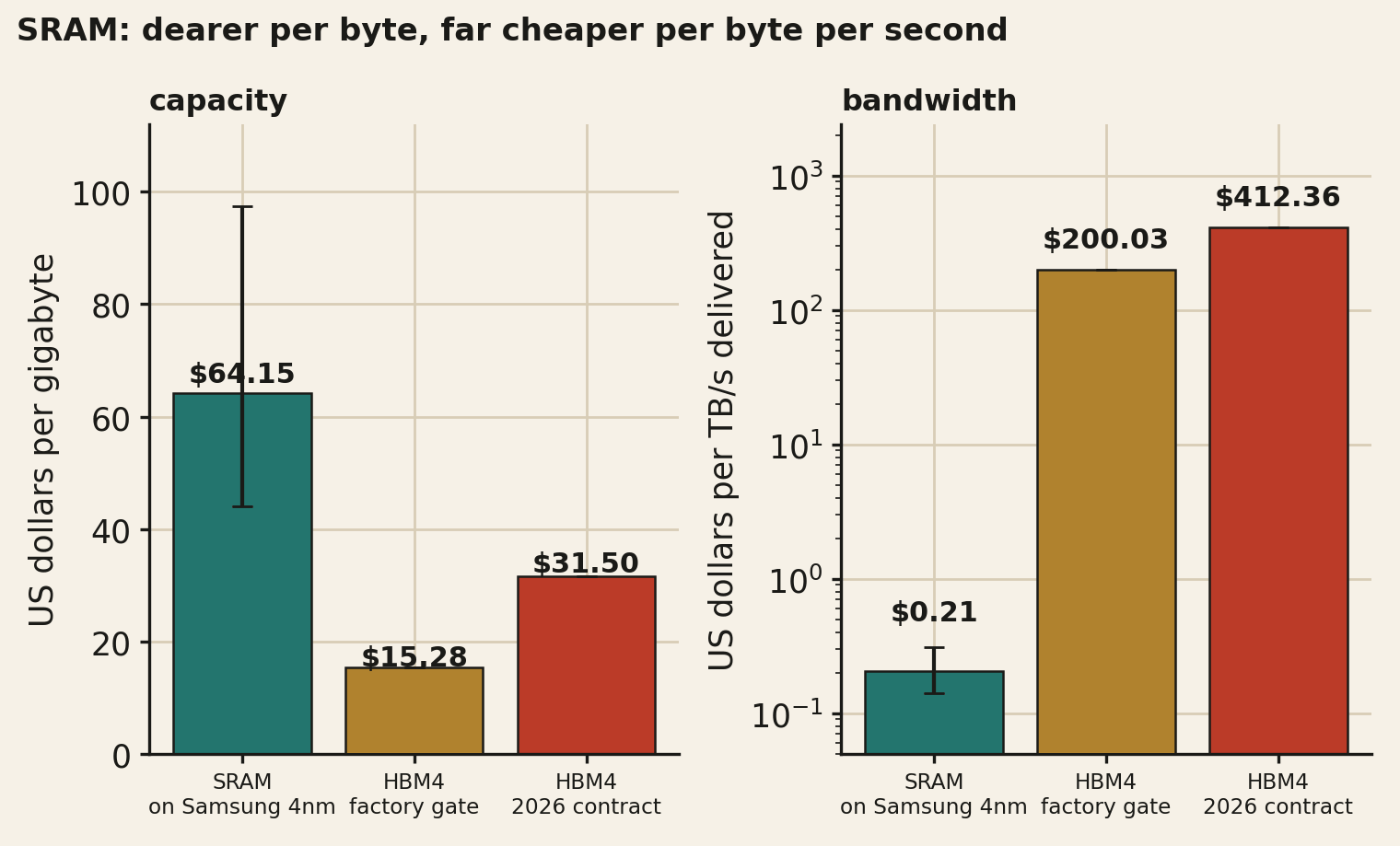
The 512 mebibyte array delivers 156 TB/s, so the silicon under a terabyte per second of SRAM bandwidth costs 14 to 31 cents, centrally 21. The 288 gigabytes of HBM4 on a Rubin package delivers 22 TB/s, so the memory under a terabyte per second of HBM bandwidth costs about 200 dollars as a component and 412 under contract.
Take the corner least favourable to my argument, the dearest SRAM against the cheapest HBM, and the ratio is 642. Take the central cases and it is 974 against the component price and 2,009 against the contract price. Take the corner most favourable and it is 2,924.
There is no assumption inside any of these ranges under which the answer is less than two and a half orders of magnitude, which is the only precision the conclusion needs.
Stated the other way: the SRAM in an entire LPX rack is 5,600 to 12,500 dollars of silicon area, centrally about 8,200. The HBM4 in a single Vera Rubin NVL72 rack is 317,000 dollars as a component and about 653,000 at the price NVIDIA is projected to pay. The LPX rack has twenty five times the aggregate bandwidth.
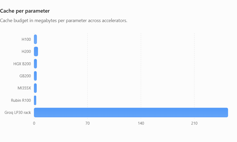
Every design decision in the LPX falls out of that one ratio. Bandwidth per byte is 3,810 times higher on the SRAM machine, which means capacity per unit of bandwidth is 3,810 times lower. A Vera Rubin NVL72 holds 20.7 terabytes. The LPX holds 128 gibibytes, which is 151 times less.
You cannot put a large model in it, you cannot put a long KV cache in it, and the only workload it can run alone is one whose entire working set is under about 137 gigabytes.
The knee
In a piece earlier this month I derived the batch size at which a decode step stops being memory bound. A decode step reads W bytes of weights and performs 2NB floating point operations, where N is the parameter count, W equals N times b bytes per element, and B is the batch. Setting compute time equal to memory time gives
B* = P · b / (2 · Bmem)
and because peak arithmetic P scales as 1/b on tensor cores, the product P·b is a generational constant. B* is invariant to precision. Running the same model in FP4 instead of FP8 doubles your token rate and moves the knee not at all.
Both sides of that ratio have to be on the same basis, which is the part that is easy to get wrong and which we both got wrong in the earlier drafts of this piece. A sparse or compressed peak divided by a real bandwidth inflates B* by the compression ratio. Every figure below is dense.
The invariance held well for two generations. H100 sits at 295, H200 at 206, HGX B200 at 292, GB200 and MI355X at 312. All five re-derive here from datasheet FP8 dense throughput and published HBM bandwidth, so the plateau is a result rather than a citation.
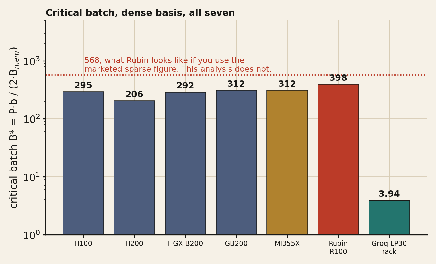
Rubin is where the basis matters. NVIDIA markets the R100 at 50 PFLOPS of NVFP4 inference, and that figure is not dense. SemiAnalysis reports that NVIDIA brands 50 PFLOPS as the inference number while 35 PFLOPS of NVFP4 is the dense one, and that the five times over Blackwell claim compares compressed FP4 against dense FP4. Their Rubin CPX analysis puts the same part at 50 sparse and 33.3 dense on a three to two ratio.
NVIDIA’s own rack table settles it. The NVL72 is published at 3,600 PFLOPS of NVFP4 inference, 2,520 of dense NVFP4, and 1,260 of dense FP8.
Divide by 72 and the per package figures are 50 marketed, 35 dense NVFP4, and 17.5 dense FP8. The ratio between the marketed and the dense number is 3,600 over 2,520, which is ten to seven.
Both dense figures give the same answer, as they must, since P scales as 1 over b: 35 PFLOPS at half a byte and 17.5 at one byte are the same product. Against 22 TB/s, B* is 398. The SemiAnalysis route through the three to two tensor core ratio gives 378. Had I used the marketed 50, I would have got 568, which is exactly the ten to seven too high.
So the knee moved 1.36 times over HGX B200, and not 1.94. That is a smaller claim than the one I started with and it is the one the arithmetic supports. To run a Rubin package at the batch where its arithmetic is fully occupied you need 398 concurrent sequences resident on it, against 292 on Blackwell.
One refinement falls out of the same correction. The invariance is not across all precisions on this part. SemiAnalysis reports that the third generation Transformer Engine doubles tensor core width for FP4 and FP8 only, leaving BF16 and TF32 to scale about 1.6 times. P·b is therefore no longer one constant: B* is 398 at FP8 and at NVFP4, and near 164 at BF16. On Blackwell it was 292 at all three. Anyone still serving in BF16 is on a machine with a very different knee from the one on the slide.
An LPX rack is rated at 315 PFLOPS of FP8 across 40 PB/s of SRAM. B* equals 3.94. Per chip the answer is identical, because the ratio is scale invariant: 1.23 PFLOPS against 156 TB/s gives the same 3.94.
The ratio between the two machines is 101.
The benchmark model is not incidental
Gemma 4 31B was released by Google DeepMind on 2 April 2026 under Apache 2.0 license. Its configuration is public: 60 layers, of which 50 are sliding window attention with a window of 1,024 and 10 are full global attention, 32 query heads, 16 KV heads, a head dimension of 256 in the sliding layers and 512 in the global ones.
The Gemma 4 technical report describes two memory optimisations on the global layers. Keys are re-used as values, and position is encoded with p-RoPE at p equal to 0.25. It then states that this reduces the global KV cache by 37.5 percent, without saying how.
That constant is derivable, and deriving it tells you what is actually stored. If you keep K and V separately you store 2d bytes per head per token. If values equal keys you would store d, a 50 percent cut.
But K carries rotary position and V must not, so the shared tensor can only be the unrotated part. With p-RoPE only a fraction p of the head dimension is rotated, so what you keep is the full unrotated tensor plus a rotated copy of the p fraction:
stored / baseline = d(1 + p) / 2d = (1 + 0.25) / 2 = 0.625
which is a 37.5 percent reduction, exactly. The residual against the published figure is zero. So the global layers store 1.25 tensors where a conventional model stores 2.
One step here is entirely from me and Lorenzo Tettamanti and not the config’s. The published file gives 16 KV heads, a head dimension of 256 and a global head dimension of 512, and does not state a separate global head count.
I take it to be 8, on the reasoning that 8 heads at 512 is the same 4,096 element width as 16 at 256, which is the pattern the 26B variant follows and the only one under which the report’s 37.5 percent lands on a round byte figure. The whole cache number below rests on that inference, so it is marked as an inference in the dossier rather than buried here.
I flag one disagreement. Several community analyses of this model use 8,192 bytes per token per global layer, which corresponds to a clean 50 percent reduction and omits the rotated copy. The report’s own 37.5 percent implies 10,240. I use the report.
Run the cache arithmetic at 100K of context and the sliding layers contribute 0.84 gigabytes, capped by their 1,024 token window and therefore constant in context length, while the global layers contribute 10.24. The total is 11.1 gigabytes. A conventional model with the same head count and 60 full attention layers would need 98.3. The hybrid saves 8.87 times at 100K and 9.31 times at the model’s full 262,144.
Weights plus cache at 100K in FP8 is 41.8 gigabytes, which is 30.4 percent of the LPX rack’s 137.4 gigabytes. In BF16 it is 52.7 percent. The benchmark fits with room to spare, and it fits because Gemma 4 is close to the best case a 128 gibibyte SRAM machine could ask for: a dense model small enough to shard 256 ways, with an attention design that caps its own cache growth.
Work out what would not fit. With 100K of its own cache resident, the largest dense model an LPX rack holds is 126 billion parameters at FP8 or 253 billion at FP4.
The two trillion parameter figure NVIDIA quotes is 1,000 gigabytes at FP4, or 7.3 racks of SRAM, and the figure in their blog that carries it is labelled a projection of a scaled up GPT-OSS, not a measurement. That is honest labelling on their part and I want to repeat it rather than let it blur.
The term the formula drops
Here is where we have to correct our own framing, because the formula above is incomplete and the incompleteness is not small.
B* comes from a decode step that reads W bytes of weights and performs 2NB flops. That accounting is right only if the KV cache is negligible. It is not.
At batch B and context S a decode step reads W plus B times KV(S) bytes, because every resident sequence’s cache is read once per token, while the flops that batching amortises are still only 2NB. Attention’s own flops scale with context exactly as its bytes do, so attention has fixed arithmetic intensity and never becomes compute bound at any batch.
Restore the term and set compute time equal to memory time:
2NB / P = (W + B·KV) / Bmem
B (2N·Bmem/P − KV) = W
B* = b / (2·Bmem/P − KV/N)
This reduces to the weights-only form when KV goes to zero. It also has a pole. When KV per sequence reaches 2·Bmem/P per parameter, the denominator vanishes and B* goes to infinity: past that context, no batch size makes the machine compute bound, because each additional sequence adds more memory traffic than it adds amortisable arithmetic.
Call that the saturation context. It is the number I should have led with.
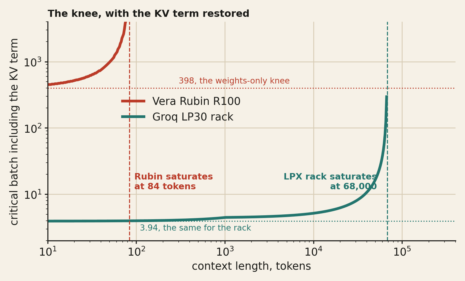
For a Rubin package the headroom is 2.51 millibytes of KV per parameter, which on a 30.7 billion parameter model is 77 megabytes. Gemma 4’s cache passes 77 megabytes at 84 tokens of context. Eighty four. Past that, a Rubin GPU serving this model is memory bound at every batch size there is.
For the LPX rack the headroom is 254 millibytes per parameter, or 7.8 gigabytes of cache, which Gemma 4 reaches at about 68,000 tokens. The ratio between the two saturation contexts is 811, not the 101 that the weights-only knees give, because the sliding window caps 50 of the 60 layers and makes the relationship nonlinear.
One input to that carries more weight than I would like. The published config gives 16 KV heads and a 512 dimension global head, but does not state a separate global head count, and I read it as 8 on the constant width argument above.
Take the literal 16 instead and the cache doubles to 21.3 gigabytes at 100K, Rubin’s saturation moves only from 84 tokens to 75, and the LPX’s halves from 68,000 to 34,000. The ratio becomes 451 rather than 811. Every qualitative claim survives that swing and the LPX figure is good to within a factor of two, which is the honest precision on it.
Run it across every machine in the table and the picture is worse than a two way comparison suggests.
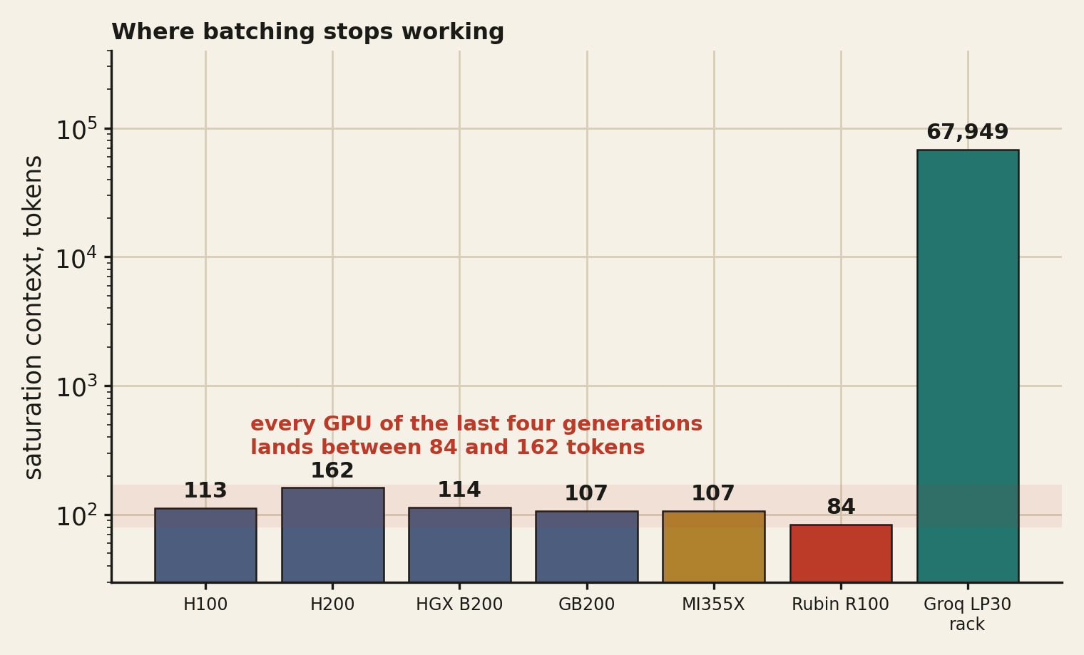
Every GPU lands inside a hundred token band, across four years and three process nodes. The trend within it runs the wrong way. H200 is the best of them at 162 tokens, because it added bandwidth without adding arithmetic. Rubin is the worst at 84.
Four generations of progress moved the saturation context down 26 percent, which is the same statement as saying that compute has outrun bandwidth, made in units that matter for serving rather than in FLOPS.
So the honest version of this article’s central claim is not that the LPX has a lower knee. It is that at the context lengths the machine is sold for, the LPX still has a knee and no GPU does. Not this one, and not any of the five before it.
What that does to the tax
The interactivity tax I was about to compute, hardware carried per token at batch b against the same machine at its knee, doesn’t survive this. Below saturation, throughput is linear in batch.
Above it, throughput saturates at Bmem divided by KV no matter how much batch you add. At 100K of context both machines are above saturation, so the binding constraint stops being the knee and becomes capacity.
Work it through at 100K. Gemma 4’s cache is 11.08 gigabytes per sequence. A Vera Rubin NVL72 holds 20.7 terabytes, so after weights it fits about 1,869 concurrent sequences and tops out near 143,000 tokens per second for the rack. An LPX rack holds 128 gibibytes, so after weights it fits 9.6 sequences.
Now compare each machine at its own best point. The Rubin rack at 1,869 sequences produces 143,000 tokens per second and gives each user 76. The LPX rack, measured, produces 11,000 tokens per second and gives each user 3,431. The GPU rack makes 13 times the tokens. The LPU rack makes each user’s tokens arrive 45 times faster.
That is the trade, at one context length, with no marketing basis anywhere in it. And it is a far smaller hardware-amortisation story than the one I started with: going from the LPX’s operating batch of 3.2 up to the Rubin rack’s capacity limit improves tokens per rack-second by 1.86 times, not by 124. The weights-only figure overstates the tax at 100K context by a factor of 67.
Which leaves the LPX’s case resting almost entirely on latency rather than on hardware amortisation. That happens to be what the rest of the arithmetic says too.
Where the token actually goes
Here is where the arithmetic stops flattering the machine.
Gemma 4 31B has 30.7 billion parameters. At FP8 that is 30.7 gigabytes of weights, and at 100K of context its KV cache is 11.1 gigabytes, which I derive below. A decode step at batch one reads 41.8 gigabytes.
At 40 PB/s that takes 1.04 microseconds, which is a roofline of 957,422 tokens per second.
The measured figure is 3,431. The gap is 279 times.
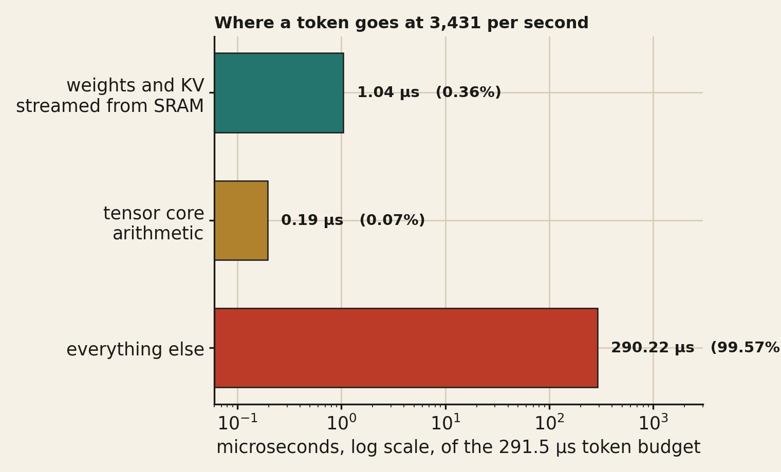
The token budget is 291.5 microseconds. Streaming the weights and the cache accounts for 1.04 of it. All of the arithmetic, 61.4 gigaflops at 315 PFLOPS, accounts for 0.195.
Together, every operation that does useful work occupies 0.43 percent of the budget. The other 99.57 percent is synchronisation, scheduling, and the fixed cost of moving small tensors between chips.
This is not a criticism of the design, at all. It is what NVIDIA’s own engineers say the machine is for. Their blog post on the benchmark spends its technical section on a single equation, the time to move data between two chips as A plus N over B, and argues that at high interactivity the fixed startup cost A dominates because N is tiny. My arithmetic says they are right.
How far it can be decomposed depends on the mapping, and here I have to withdraw something. An earlier version of this piece assumed pure tensor parallelism across all 256 chips with two all-reduces per layer, and derived a per-collective cost from it.
Groq’s own documentation says the machine runs pipeline parallelism layered on top of tensor parallelism: a layer is split across a group of chips and layer groups are pipelined. Without the mapping, the collective count is unknown and the per-collective figure was not supportable.
What survives does not need the mapping. Layers are a sequential dependency chain however each one is placed, so the per-layer budget is 4.86 microseconds. Streaming that layer’s share of weights and cache is 17 nanoseconds of it. Its arithmetic is 3 nanoseconds. Moving the activation between chips once, 8.2 kilobytes at the chip’s 1.34 terabytes per second of link bandwidth, is 6 nanoseconds. Add all three and you have accounted for 0.5 percent of the layer.
The pipeline structure makes this worse rather than better at the operating point being advertised. Pipelining buys throughput by overlapping stages across concurrent work; it buys a single stream nothing, because one token must still traverse every stage in order. At a concurrency of three, a 256 chip pipeline is running close to empty and paying its full depth on every token.
One caveat I cannot resolve without hardware. The 3,431 figure is an end-to-end median measured by Artificial Analysis over a network, so some unknown fraction of the 291.5 microseconds is client side and never touches the rack.
My decomposition therefore bounds the machine’s internal latency from above rather than measuring it. The direction of the error makes the machine look worse than it is, and the conclusion, that this is a latency product and not a bandwidth product, survives any plausible correction.
The consequence for anyone sizing hardware is direct. At batch one this rack achieves a model FLOP utilisation of 0.067 percent. At its measured concurrency of 3.21 it achieves 0.21 percent. You are buying 315 PFLOPS and 40 PB/s in order to use two thousandths of them, and the entire value proposition is that the two thousandths arrive quickly.
There is one more gap worth naming. At 100K of context the rack has room for 9.6 sequences, and if it ran all of them at the advertised 3,431 tokens per second it would produce 33,000 tokens per second rather than the 11,000 NVIDIA quotes.
It is leaving three times its own capacity ceiling unused. That is what a pipeline looks like when filling it would cost the latency the product is sold on.
The context tax
Artificial Analysis ran the same suite at 10K and at 100K on 20 August. The LPX went from 3,382 to 3,431 tokens per second, which is faster at ten times the context. The fastest public endpoint went from 1,402 to 870.
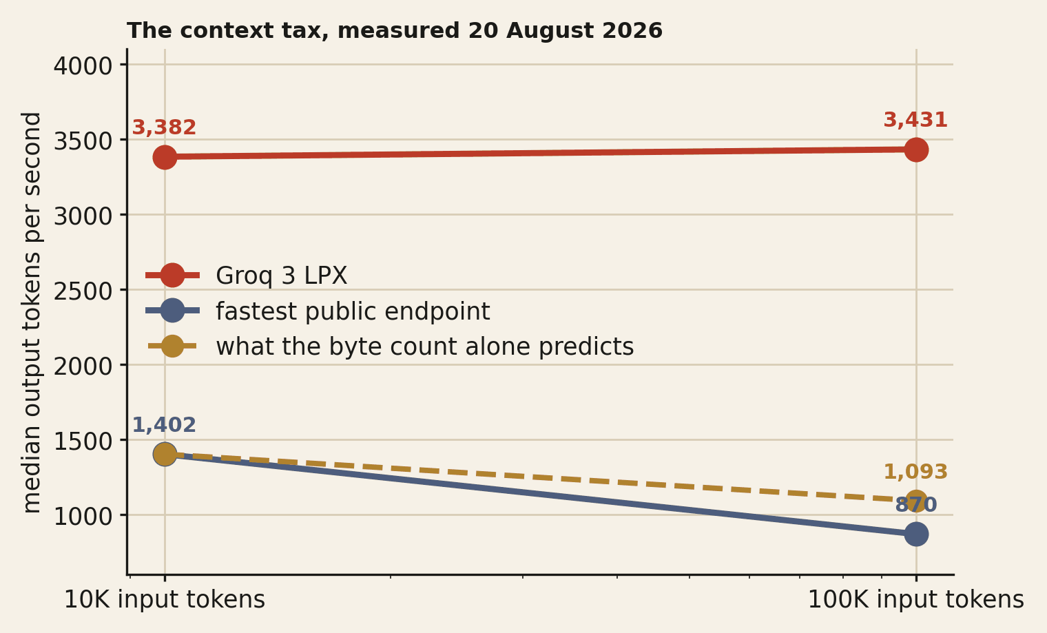
My byte model says a decode step at 100K reads 1.283 times what it reads at 10K, because the sliding layers are window-capped and only the ten global layers grow.
A purely bandwidth bound machine would therefore slow by 22.1 percent. The LPX moved by plus 1.4 percent, which is inside measurement noise and confirms directly that bandwidth is not what limits it. The public endpoint slowed by 37.9 percent, which is 1.72 times what the byte count alone predicts.
That excess is the part I find most useful for practitioners. Whatever is costing the GPU endpoint an extra 16 points of throughput at long context is not the KV bytes. It is paging, chunked prefill interference, attention kernel behaviour at low batch, or a scheduler shrinking the effective batch as sequences lengthen.
Those are software problems with software fixes, and they are roughly as large as the hardware difference the whole LPX programme exists to address.
Who the four times is actually against
NVIDIA’s headline is that the LPX produced 3,431 tokens per second against 870 for the next fastest public endpoint, a factor of 3.94. It does not name the endpoint.
ServeTheHome’s live coverage from the session says the comparison looks like a Cerebras CS-3, and the provider data supports that: Cerebras is the fastest benchmarked provider for this model at 1,191.7 tokens per second, and it is the only one whose figure is in the right range to degrade to 870 at 100K.
If that identification is right, then NVIDIA’s four times is against another SRAM machine. Against the fastest GPU-served endpoint for the same weights, which is Modular’s NVFP4 deployment at 233 tokens per second, the LPX is 14.7 times faster. Cerebras is itself 5.1 times faster than that endpoint.
We both think the correct reading is not that NVIDIA beat the field. It’s that there are two regimes, that the SRAM machines occupy one of them and every GPU occupies the other, and that NVIDIA has just spent 20 billion dollars to be present in both.
The interesting comparison in the deck is not the bar chart. It is the pareto curve NVIDIA showed at Hot Chips, where its own presenter conceded that total throughput efficiency falls as more work moves to the LPUs, and that GPUs remain the efficient choice whenever latency is negotiable.

If you are serving models rather than buying them
A few things in the arithmetic above are actionable without any new hardware.
The largest is the context tax. The fastest public GPU endpoint loses 37.9 percent of its throughput going from 10K to 100K of context, and the decode byte count only accounts for 22.1 of those points. The remaining 16 points are software: paging, chunked prefill interference, attention kernel behaviour at low batch, or a scheduler quietly shrinking the effective batch as sequences lengthen. That gap is roughly as large as the hardware difference this entire programme exists to address, and it is available to anyone willing to profile a long-context decode path this week.
The second is that above the saturation context, batching stops buying throughput. Every serving guide tells you to raise batch until you are compute bound. On a Rubin package running a 31 billion parameter model with Gemma 4’s attention geometry, that point is at 84 tokens of context, which means it does not exist for any real workload. What batch still buys above saturation is capacity utilisation, not arithmetic utilisation, and the ceiling is memory bandwidth divided by cache bytes per sequence. For this model on an NVL72 that ceiling is about 143,000 tokens per second and no scheduler setting will beat it.
The corollary is that quantising the KV cache is worth more than quantising the weights once you are above saturation, because the ceiling is set by cache bytes. Halving KV precision raises the ceiling by two. Halving weight precision moves it not at all.
The third is where to look for cache savings. Gemma 4’s hybrid attention makes its cache 8.87 times smaller at 100K than a conventional design with the same head count, and almost all of that comes from ten global layers being the only ones that grow with context. If you are sizing a KV budget, the layer type distribution matters more than the head count, and a model with a 5:1 local to global ratio is a fundamentally different capacity problem from one without.
What the market pays for speed
Gemma 4 31B is a very good instrument for a price question because the weights are identical everywhere. Thirteen or so providers serve the same Apache 2.0 checkpoint. Any price difference between them is a price on the machine, not on the model.
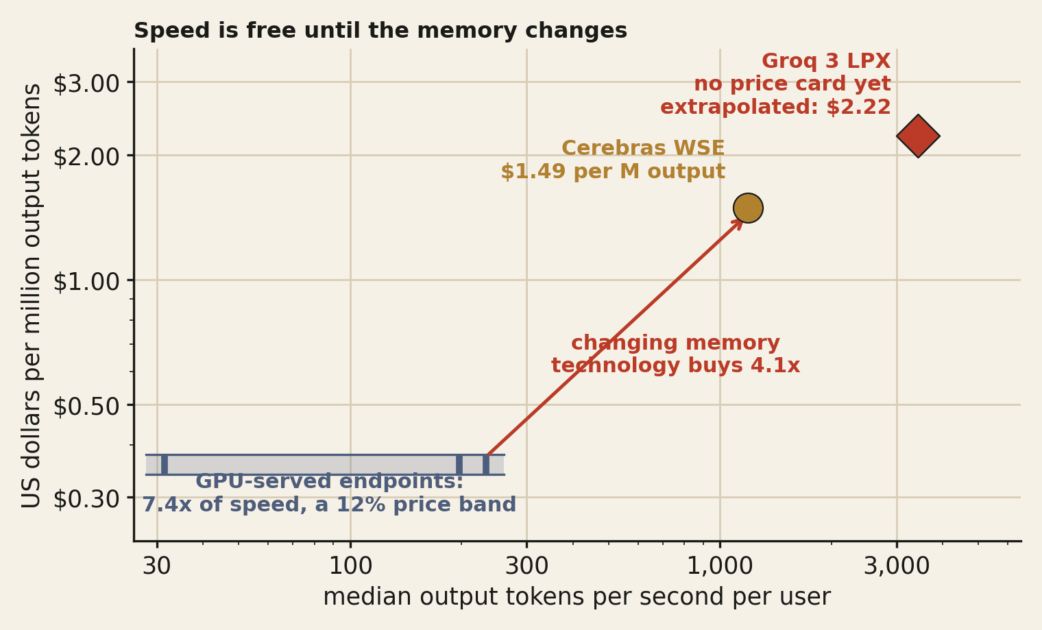
The GPU-served providers span 31.5 to 233 tokens per second, a factor of 7.4. Their output prices are 0.34 at CoreWeave, 0.38 at DeepInfra, and 0.34 to 0.35 through OpenRouter: a band of 12 percent. Fitting an elasticity to that gives 0.056, which for practical purposes is zero. Inside the GPU regime, seven times the speed is free.
The only price step in the market is at the regime boundary. Cerebras charges 0.99 per million input tokens and 1.49 per million output, against 0.08 and 0.38 at the cheapest tracked provider.
That card is confirmed rather than assumed: Artificial Analysis publishes a blended rate of 1.04 for this model on Cerebras, and 0.99 and 1.49 reproduce it exactly under their seven to two to one weighting with no cache discount. That is 4.1 times the commodity output price for 5.1 times the fastest GPU speed, and 12.4 times on input.
Two things follow that we didnt expect before running the numbers.
First, the elasticity computed across the full range, 0.376, is an artifact of fitting to the two extremes. It is an upper bound on what speed is worth, not a description of the market, because the intermediate points do not lie on it. Anyone modelling a fast inference business off a smooth speed premium is modelling a curve that does not exist. What exists is a commodity floor and one occupied premium tier.
Second, input tokens carry the larger premium. Cerebras marks up input 12.4 times and output 3.9 times. That is the opposite of the intuition that a fast decoder should charge for decode, and it makes sense the moment you remember that a machine with no DRAM has to hold the prefill working set somewhere expensive.
Extrapolating the two-point curve to the LPX’s 3,431 tokens per second, which is 2.88 times Cerebras, gives an implied price near 2.22 dollars per million output tokens and 2.06 on input.
NVIDIA has not published a price card, so this is the market’s shape and not the company’s intention. I use it as a scenario, and I flag that it rests on the same two-point fit I just described as an upper bound.
Where the revenue actually sits
Now put that against the workload NVIDIA chose to sell the machine with. From their blog: an agentic coding turn in which the model reads hundreds of files, exceeds 100K of context, and generates 5,000 tokens of reasoning and output.
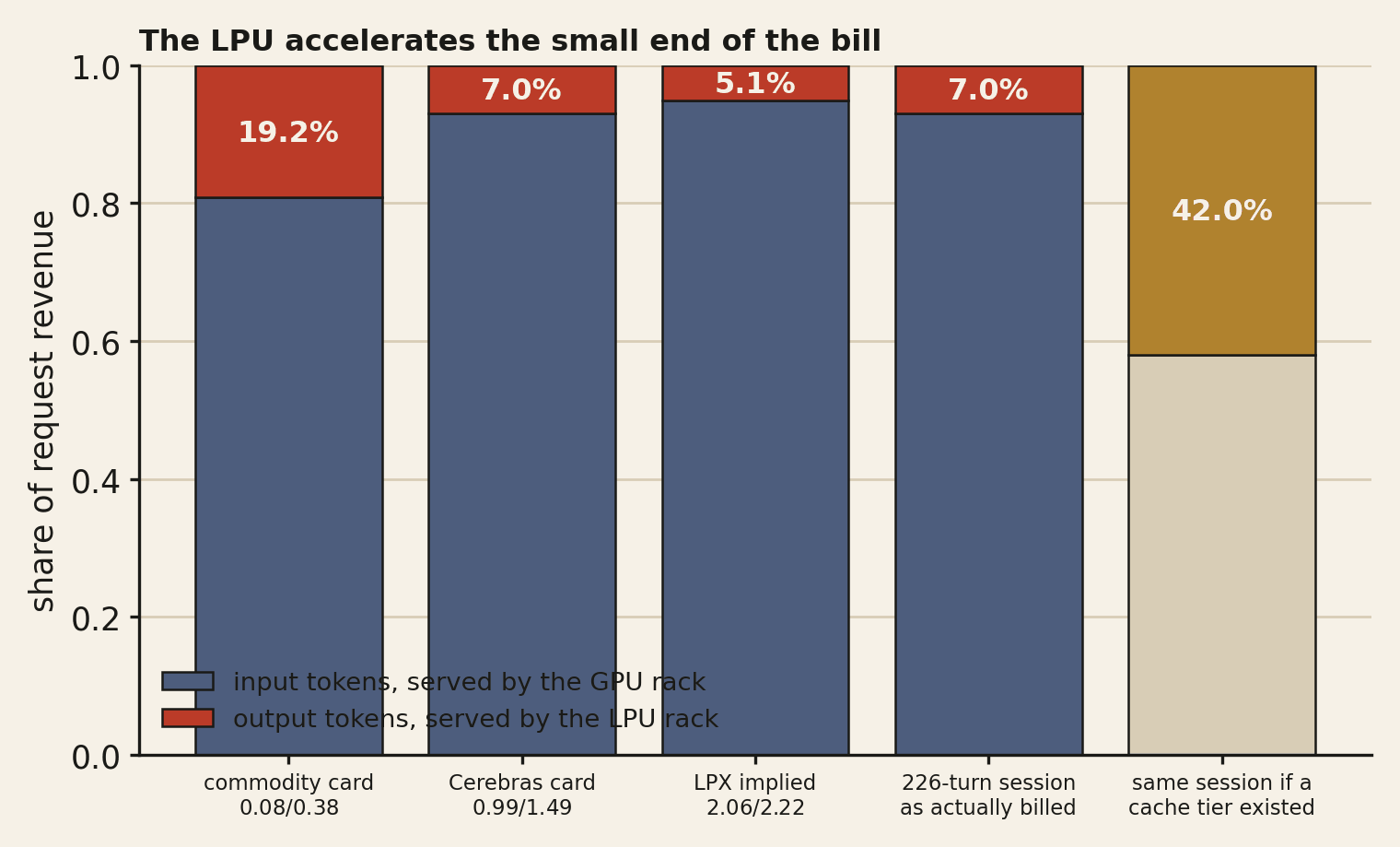
Price that turn on the commodity card and 19.2 percent of the revenue is output tokens. Price it on the Cerebras card and 7.0 percent is. Price it on the extrapolated LPX card and 5.1 percent is.
This matters because of how the rack is wired. In all three co-execution configurations NVIDIA describes, prefill happens on the Vera Rubin GPUs. In prefill-decode disaggregation the GPU rack hands over the KV cache once per turn.
In attention-FFN disaggregation the GPU computes attention and holds the cache in DRAM while the LPUs run the feed forward layers. In external-drafter speculative decoding the LPUs run a draft model and the GPUs verify. In every case the input tokens, which are 81 to 95 percent of the revenue in NVIDIA’s own example, are billed against work the GPU rack does.
The LPU accelerates the small end of the bill and all of the latency. For a product whose promise is user experience that is exactly right. For a claim of ten times more revenue per watt it’s a great problem, and NVIDIA’s own footnote on that claim says as much: the figure is projected from an estimated cost-per-million-tokens tiered pricing model. It is a statement about a price card that does not exist yet.
I wanted to offer prefix caching as the counterweight here, and the arithmetic will not let me. Agentic sessions reuse their context, and NVIDIA’s own figure one shows a session growing across 226 turns.
Bill the first turn’s input at full rate and later turns at a tenth, and the output share rises from 7 percent to 42, which would be a different business and the business the LPX is actually for.
But the provider in question does not sell that. Artificial Analysis publishes a blended rate of 1.04 dollars per million for this model on Cerebras, and 0.99 in with 1.49 out reproduces it under their seven to two to one weighting only if cache hits are billed at the same 0.99 as fresh input.
Solve for the cache price and it comes back at exactly 0.99. There is no discount. So the 226 turn session bills at a 7.0 percent output share, the same as a single turn, and the counterweight I was reaching for is hypothetical on every endpoint I can price.
If a fast tier ever does offer cache pricing, the 42 percent figure is what it would look like, and that is the number to watch. It is also a business in which the cache has to live somewhere, and the somewhere is HBM on the GPU rack, which is the component under the 279 billion dollar commitment.
What the rack has to cost
11,000 tokens per second is 347 billion tokens per rack-year at full utilisation. At 70 percent utilisation over a four year life, at the extrapolated 2.22 dollars per million output tokens, the rack grosses 2.16 million dollars.
That is the ceiling on what it can cost, before power, before the paired Rubin capacity that does its prefill, and before anyone earns a margin. At the Cerebras card of 1.49 it is 1.45 million. At commodity output pricing of 0.38 it is 369,000 dollars, which would not pay for the rack’s power.
NVIDIA does not publish an LPX rack power figure, which means the 35x throughput per megawatt and 10x revenue per watt claims cannot be checked by anyone outside the company. I would treat both as unverified until a number appears. Everything else in the deck was specified to three significant figures.
So the arithmetic closes only under a conjunction: the premium tier has to hold at nearly three times Cerebras’s speed, the workload has to be cached enough that output is a real share of the bill, and the rack has to land under roughly two million dollars. None of those is absurd. All three have to be true at once.
What we really think this is about
Both of our reading is that the LPX is not primarily a product. It’s a hedge on a component price.
NVIDIA has committed 279 billion dollars to memory, front loaded into three years, with a gross margin guide already bending under it. Memory is the input it cannot substitute, cannot second source beyond three vendors, and cannot make itself.
In that position, owning a machine whose bandwidth comes from a 4nm logic wafer rather than a stacked DRAM package is worth something independent of whether the machine sells well, because it is the only lever that converts a purchased input into a manufactured one.
The Rubin CPX supports this reading. It was announced in September 2025 as a GDDR7-based accelerator for the context phase, and it has quietly left the roadmap, displaced by the LPX. GDDR7 is still DRAM you have to buy. SRAM is area you already pay TSMC or Samsung for.
The thing I keep returning to is that the entire architecture is legible from a single number.
3,810× more bandwidth per byte, combined with bandwidth that is 642–2,924× cheaper per unit and memory that is 1.4–6.4× more expensive per byte, pushes the saturation context out by a factor of 811×. From there, the rest of the architecture follows almost inevitably.
It favors a small model. It puts attention back on the GPU because the cache cannot fit. It makes a hybrid-attention model, whose cache is roughly nine times smaller than a conventional one, the natural benchmark. It requires tensor parallelism across 256 dies. And it ultimately demands a compiler capable of scheduling 320-byte transfers to the clock cycle, because at batch three, the fixed cost of moving the data is effectively the cost of generating the token itself.
That is what makes the machine interesting. These are not a collection of independent design choices. They are consequences of the same economic constraint propagating through the stack.
It is a coherent machine because it is solving a procurement problem.
Where this analysis might be wrong
The concurrency of 3.21 comes from dividing a rack throughput figure by a per-user figure that may have been measured at a different operating point.
If the 11,000 tokens per second is a peak throughput number at relaxed latency rather than the aggregate at 3,431 per user, then the true concurrency at the advertised speed is lower, not higher, and the interactivity tax argument gets stronger while the revenue arithmetic gets worse. I have used the reading least favourable to my own conclusion.
The SRAM cost model uses a 5nm class bit cell on a Samsung 4nm part. If Samsung’s density is materially worse, the per-gigabyte figure rises and the per-terabyte-per-second figure rises with it. It would take roughly a factor of 900 to change the sign of the bandwidth comparison, so the conclusion is not sensitive, but the 66 dollars per gigabyte is a model and not a measurement.
The identification of Cerebras as the unnamed baseline is inference from a third party’s live blog plus provider data. If the 870 figure is some other endpoint, my point about the four times being an SRAM-to-SRAM comparison weakens.
The 28 dollar per gigabyte reconciled memory price rests on a GPU average selling price band I chose. Narrow the band and the answer moves. I reported the range rather than the point for that reason, and the fact that it lands inside the published analyst band is a check on the method, not a proof of the point estimate.
And the price extrapolation is the weakest link in the piece. I have one premium data point. One point does not make a tier.
The session revenue model originally billed repeat input at a tenth of list, assuming a prefix cache discount, and reported a 42 percent output share on that basis. My own price check rules it out: the published blended rate only reconciles if cache hits cost the same as fresh input. The 42 percent is now labelled hypothetical and the measured case is 7.0.
The latency decomposition originally attributed the unexplained 99.5 percent to a specific count of tensor parallel collectives. Groq documents pipeline parallelism on top of tensor parallelism, which makes the collective count a function of a mapping I do not have, so that attribution is gone and only the topology independent per-layer budget remains.
The larger of the two things I got wrong is in the section above: I built the argument on a critical batch formula that drops the KV term, which is fine for comparing machines and wrong for describing serving.
Restoring it moved the interactivity tax at 100K context from 124 times to 1.86 times and replaced the whole framing with the saturation context. I have left the derivation of the error in the text rather than quietly fixing the numbers, because the weights-only formula is in wide circulation and the pole is the part nobody mentions.
The other one, worth naming rather than paraphrasing, is that the first version of this piece computed Rubin’s critical batch from the marketed 50 PFLOPS NVFP4 figure and every other machine’s from a dense one.
That produced 568 instead of 398, a break of 1.94 times instead of 1.36, and an interactivity tax of 177 instead of 124. It is the same denominator mixing I have criticised in other people’s analysis, and the harness did not catch it because the harness only checked that the arithmetic followed from the constants, never that a constant meant what its name said. Every arithmetic figure now carries a declared basis and the code refuses to divide across a mismatch.
The LP30 rack’s 315 PFLOPS carries no stated basis either. I read it as dense because the LP30 is a deterministic machine with no published structured sparsity mode. If it turns out to be a sparse figure, B* halves to 1.97 and every argument here gets stronger, so the reading I chose is again the unfavourable one.
Five dated predictions
NVIDIA publishes an LPX rack power figure before the end of FY2027, and the 35x per megawatt claim is restated against a specific model and batch when it does.
The first public LPX price card, whenever it appears, prices input tokens at a larger multiple of commodity than it prices output tokens, following the Cerebras shape rather than the intuitive one.
Supply and capacity commitments fall below 200 billion dollars within four quarters, because the three year front loading in this table is a one time securing of a position rather than a new run rate.
By the end of 2027 at least one frontier open weights model ships with an attention design chosen explicitly so that its cache fits in an on-package or on-die SRAM budget, and the release notes say so.
The next NVIDIA datacenter generation after Rubin lands with a dense B* above 450. Rubin moved the knee 1.36 times in one step while HBM4 bandwidth grew 2.75 times, and the compression engine is the tell: when a vendor starts marketing a compressed peak, the dense ratio is the number under pressure.
Corrections
This is the final version of this massive research project. What changed so far during the journey:
The headline number. Rubin’s critical batch was computed from the marketed 50 PFLOPS NVFP4 figure, which is compressed rather than dense, while every other machine used a dense figure. B* was 568 and is 398. The generational break was stated as 1.94 times and is 1.36. The interactivity tax was 177 and is 124. The ratio between the two machines was 144 and is 101.
The fifth prediction has been replaced. It said no generation through 2028 would bring B* under 400. The corrected figure is 398, so it was false on arrival.
A secondary source contradicted a primary one. An earlier draft said Data Center Networking grew 138 percent. The CFO commentary has no networking line and 138 percent belongs to the AI Clouds, Industrial and Enterprise segment.
An inference was presented as a fact. The count of 8 global KV heads in Gemma 4 31B is not in the published config. It is now disclosed where it is used and carried at tier C.
A mislabelled quantity. The 4,096 in the collective payload calculation is the KV width, not the hidden size, which is not published for this checkpoint.
A figure caption overclaimed. Figure 5 said the band spanned providers with both a price and a speed published. Only one provider publishes both.
Five historical B* values were imported rather than derived. All five now re-derive inside the harness from datasheet dense FP8 and published bandwidth.
The HBM4 price was on the wrong basis. Version 2 used 15.28 dollars per gigabyte throughout and called it a contract price. It is a factory gate component price. The contract price projected for 2026 is 31 to 32 dollars per gigabyte to NVIDIA and 35 to 36 to other buyers. Both bases are now shown. The bandwidth advantage of SRAM widens from 914x to a range of 914x to 1,885x, and the capacity penalty narrows from 4.3x to a range of 2.1x to 4.3x.
The triangulation is now checked against the right number. The reconciled 28.2 dollars per gigabyte was compared to the factory gate figure and reported as 1.85 times it. Compared to the published analyst contract price it is within 11 percent, from two methods sharing no inputs, which is a far stronger result than the one originally claimed.
Two unverifiable attributions were removed. A job title given for the Hot Chips presenter that no source in hand supports, and an implied claim that the Rubin package carries eight HBM4 stacks, which 288 gigabytes does not uniquely determine.
The dense figure is now confirmed from NVIDIA’s own rack table rather than from a single outlet: 3,600 PFLOPS NVFP4 inference against 2,520 dense NVFP4 and 1,260 dense FP8, which is ten to seven and 17.5 PFLOPS per package.
The session revenue model assumed a cache discount the provider does not offer. It billed repeat input at a tenth of list and reported a 42 percent output share. Solving the published blended rate for the cache hit price returns exactly the input price, so there is no discount. The measured case is 7.0 percent and the 42 is now labelled hypothetical. The error ran in the direction that flattered the argument being made.
The one tier C input carrying a headline now ships with its sensitivity. The global KV head count is inferred, not published. Under the literal reading the LPX saturation context halves to 34,000 and the ratio falls from 811 to 451. Both are in the text.
The latency decomposition assumed a topology that is not documented. It attributed the unexplained part of the token budget to a specific count of tensor parallel collectives across all 256 chips. Groq documents pipeline parallelism layered on top of tensor parallelism, so the collective count depends on a mapping that is not published. The per-collective figure is withdrawn. What remains is the per-layer budget of 4.86 microseconds, of which streaming, arithmetic and one chip-to-chip handoff together account for 0.5 percent, and that holds under any mapping.
The rack break-even was given as a point. It now runs as three scenarios from 369,000 dollars to 2.16 million, because the price extrapolation behind the single figure rests on a two point fit the article itself describes as an upper bound.
The central framing rested on a formula that drops the KV term. The standard critical batch B* = P·b/(2·Bmem) assumes a decode step reads only weights. Restoring the cache term gives B* = b / (2·Bmem/P − KV/N), which has a pole. Past the saturation context no batch makes the machine compute bound. For Gemma 4 31B that is 84 tokens on a Rubin package and 68,000 on an LPX rack. The interactivity tax at 100K context falls from 124 times to 1.86, an overstatement of 67 times, and the article is now built on the saturation context instead. The comparison between the machines survives; the framing did not.
The SRAM cost model used TSMC figures for a Samsung part. A TSMC N5 cell on a TSMC-priced wafer understated the cell area by about a quarter and overstated the wafer price by about the same, so the point estimate survived by accident rather than by method. It is now a band across cell size, array efficiency and wafer price: 44 to 97 dollars per gigabyte, centrally 64. The bandwidth advantage becomes a range of 642 to 2,924 times rather than a single figure.
The margin guide runs further than reported. Version 3 stopped at the 74.0 percent Q3 guide. On the call the CFO said margin falls to 71 or 72 percent by the January quarter before recovering to 72 or 73. The trough is three to four hundred basis points, not one hundred.
The SRAM bandwidth divisor contradicted the article’s own argument. The cost model divided by the trade press figure of 150 TB/s per die while the text argues the derived 156.25 is the correct one. Now 156.25 throughout.
The harness gained a basis guard. Every arithmetic constant declares dense or sparse, and the code refuses to compute B* or a ratio across a mismatch. This is the check whose absence caused the first error.