



Introduction
Full disclosure before we start: I’ve never run a program on a TPU. For most of the last decade that was the normal condition of anyone who wrote about accelerators from outside Google.
The chips lived in Google’s data centers, the papers described them a generation late, and the cloud instances were something you read about more often than something you rented.
2026 is the year that stopped being true. Anthropic is bringing up to a million TPUs online, and Broadcom has booked $21 billion of Ironwood racks for it, sold as complete systems rather than chips.
Meta signed a multi-year TPU rental in February and is negotiating to buy them for its own buildings next year. MediaTek’s TPU business is limited by how much wafer capacity it can get, not by demand. Last week Google even put four of them in orbit on a prototype satellite, running Gemma for fifteen minutes at a time. The TPU has real tenants now.
The most interesting part of the TPU, though, is not a chip. It is a 683 MB file. The runtime JAX uses to talk to TPUs ships on PyPI as a wheel called libtpu, and it contains the entire TPU compiler. That compiler will happily compile for a TPU that isn’t there.
You describe a topology, say four Ironwood chips in a 2x2x1 slice, and it hands back an executable, a cost estimate, a memory report and, if you ask with the right options, the VLIW bundles it would have sent to the chip.
The feature exists so that people can check whether a model fits on a slice before they pay for one. We used it the way we used ptxas in our pieces on NVIDIA’s compiler and on Triton: as a microscope pointed at a vendor that has never published an instruction set.
We compiled the same programs for v4, v5e, v5p, Trillium (v6e) and Ironwood (TPU7x) on a container with no accelerator at all, and read back everything the compiler was willing to say. Then we checked it against the best public description of the hardware, a five-generation retrospective by Google’s own architects (Jouppi, Lakshmanamurthy, Young and Patterson) posted in June and due in IEEE Micro.
Where the two overlap they mostly agree. The three places they don’t are Ironwood’s HBM bandwidth, the count of its matrix units, and the compute peaks of v5p and Ironwood.
A word on what kind of evidence this is. When the compiler tells us which instruction it emitted, where an array lives or which core runs a collective, that is a fact about the program it produced, and we report it as a measurement. When it tells us how many cycles something will take, that is the compiler’s model of the chip, and we label it that way every time.
The model matters on its own terms, because it is what the compiler optimizes against, but it is not a stopwatch. The public libtpu we used, version 0.0.48, does not know TPU 8t or TPU 8i. For those we have Google’s April deep dive and arithmetic.
The very short version
The compiler is on PyPI. Google’s TPU compiler ships inside libtpu, a 683 MB library, and compiles for TPUs that aren’t attached. We used it on a CPU-only container for v4, v5e, v5p, Trillium (v6e) and Ironwood (TPU7x).
The critical batch. Trillium’s is 560, the highest of any shipping accelerator we have measured. Ironwood’s is 313 on Google’s datasheet and 270 by the compiler’s own constants, in the range of NVIDIA’s H100 (295) and B200 (281).
The accumulator. In the final instruction stream for the same 1024³ bf16 matmul, Ironwood pops 1,024 results out of its matrix units and Trillium 4,096. Ironwood does no vector adds where Trillium does 3,072, and issues 80% fewer spill loads. Ironwood’s matrix instructions address a result buffer,
mrb[0]tomrb[255]; Trillium’s results come out of an unaddressed queue.Precision. By the compiler’s cycle estimates, Ironwood runs an FP8 matmul in 0.48 times the cycles of bf16 and an int8 matmul in 1.13 times. On v5e, v5p and Trillium, int8 takes 0.47 to 0.62 times and FP8 e4m3 gains little. No chip the public compiler knows runs FP4 faster than its eight-bit path.
Batch one. On v4 through Trillium, the compiler rewrites a batch-1 matmul into a vector multiply and reduction that its own cycle model prices at 2.75 to 3.50 times the matrix-unit version. One option turns the rewrite off. Ironwood doesn’t apply it.
SparseCores. On Ironwood, every collective we compiled across four or more chips ran on the SparseCores, including the ragged all-to-all that MoE dispatch uses. The one exception was the dense all-to-all. No other generation offloaded anything. TPU 8i replaces those SparseCores with an engine built only for collectives.
Storage. Arrays live in 4 KiB tiles, 128 elements wide. A single row of FP4 stores eight times its logical size. A KV cache with 64-wide heads costs twice its size in the row-major layout an attention kernel wants, and exactly its size in the layout the compiler picks when nobody asks.
Prices. On Google Cloud’s on-demand rate card, the six accelerators we priced cost $1.40 to $1.65 per TB/s of HBM bandwidth per hour, TPU or GPU. Commitments follow a fixed formula: 70% of on-demand for one year, 45% for three. The estimated anchor rate for Anthropic is 13%.
Money. Broadcom expects Anthropic to go from 1 GW of Ironwood in 2026 to 5 GW of TPU 8i in 2027 and 10 GW in 2028, and guides its AI revenue from $58 billion this fiscal year to $230 billion in fiscal 2028. Alphabet books multi-gigawatt TPU system sales in a $514 billion Cloud backlog and is raising up to $70 billion of equity for its build-out.
Compiling for TPUs we don’t own
The whole setup is one line, pip install "jax[tpu]", which in October 2026 brings jax and jaxlib 0.11.2 and libtpu 0.0.48. JAX can describe a TPU topology that isn’t attached through jax.experimental.topologies, and any program lowered against that description is compiled by the real TPU compiler inside libtpu. Each compile took from under a second to about eight seconds on a single CPU core.
The topology names are stricter than the marketing names. v4:2x2x1, v5e:2x2, v5p:2x2x1, v6e:2x2 and tpu7x:2x2x1 are accepted. v7x:2x2x1 is rejected with “Invalid TPU external name: TPU v7x”, and tpu8t, tpu8i and every other spelling of TPU 8 we tried are rejected the same way. The largest slice we asked for, tpu7x:16x16x16, came back as 8,192 devices.
import numpy as np, jax, jax.numpy as jnp
from jax.experimental import topologies
from jax.sharding import Mesh, NamedSharding, PartitionSpec as P

topo = topologies.get_topology_desc(platform="tpu", topology_name="tpu7x:2x2x1")
mesh = Mesh(np.array(topo.devices[:1]), ("x",))
spec = lambda s: jax.ShapeDtypeStruct(s, jnp.bfloat16, sharding=NamedSharding(mesh, P()))

c = jax.jit(lambda x, w: x @ w).lower(spec((8, 8192)), spec((8192, 28672))).compile()
c.cost_analysis()["optimal_seconds"]   # the compiler's roofline estimate
c.memory_analysis()                    # argument, output, temp and code bytes
c.as_text()                            # optimized HLO, one backend_config per fusion
Five kinds of output came back, and the rest of this piece is built from them. The cost analysis gives FLOPs, bytes accessed and a time called optimal_seconds. The memory analysis gives argument, output and temporary bytes and the size of the generated code.
The optimized HLO attaches a JSON backend_config to every fusion, with the tiling windows the compiler chose, an estimated cycle count, the name of the emitter that generates the code and the on-chip memory it reserves. A dump directory, enabled with XLA_FLAGS, adds 18 entries per module, including one that lists every compiler option with its value.
And two options passed through LIBTPU_INIT_ARGS, --xla_jf_dump_to and --xla_jf_dump_llo_text=true, make the compiler write every stage of its low-level backend to disk, down to the final bundles, together with a report of how many instructions of each kind a bundle can hold.
This is what one fusion looks like in the optimized HLO for a 4096³ bf16 matmul on Ironwood, trimmed to the interesting fields:
ROOT %fusion = bf16[4096,4096]{1,0:T(8,128)(2,1)} fusion(%x.1, %y.1), kind=kOutput,
  backend_config={"window_config":{"kernel_window_bounds":["512","8"],
    "output_window_bounds":["64","8"],"input_window_bounds":["64","32"],
    "estimated_cycles":"324772","iteration_bounds":["4","8","1"],
    "cost_model_type":"COST_MODEL_TYPE_CLASSIC","ml_estimated_microseconds":0,
    "buffering_level":"2"},
  "scoped_memory_configs":[{"memory_space":"1","size":"33554432"}],
  "used_scoped_memory_configs":[{"memory_space":"1","size":"31297536"}],
  "convolution_algorithm_config":{"emitter":"EmitAllBatchInSublanes"}}
The compiler split the output into 32 windows of 512 by 1,024, kept the whole K dimension of each operand window on chip, double-buffered it, reserved 32 MiB of on-chip memory and used 29.8 MiB of it, and predicted 324,772 cycles. Every number in that line is a decision someone at Google tuned, and none of it appears in the documentation.
Two fields in that config deserve a second look. cost_model_type says COST_MODEL_TYPE_CLASSIC, and next to it sits ml_estimated_microseconds, set to zero, in every matmul fusion we inspected on Trillium and Ironwood.
Google published a learned performance model for TPU programs at MLSys in 2021, and showed that it beat the production analytical model on exactly the decision this config records, tile-size selection, as well as on fusion.
TpuGraphs, a dataset for training such models, followed in 2023. In this release the slot for a learned estimate is present in every matmul fusion, and the analytical model fills in every number we report.
The 683 MB file
libtpu.so in the 0.0.48 wheel is 683,032,200 bytes, with a second 37,636,776-byte library, sdk.so, beside it.
For scale, ptxas from CUDA 13.3 is 48 MB, tileiras, the closed back end of NVIDIA’s Tile IR, is 95 MB, and Triton’s libtriton.so is 180 MB. libtpu is fourteen times ptxas.
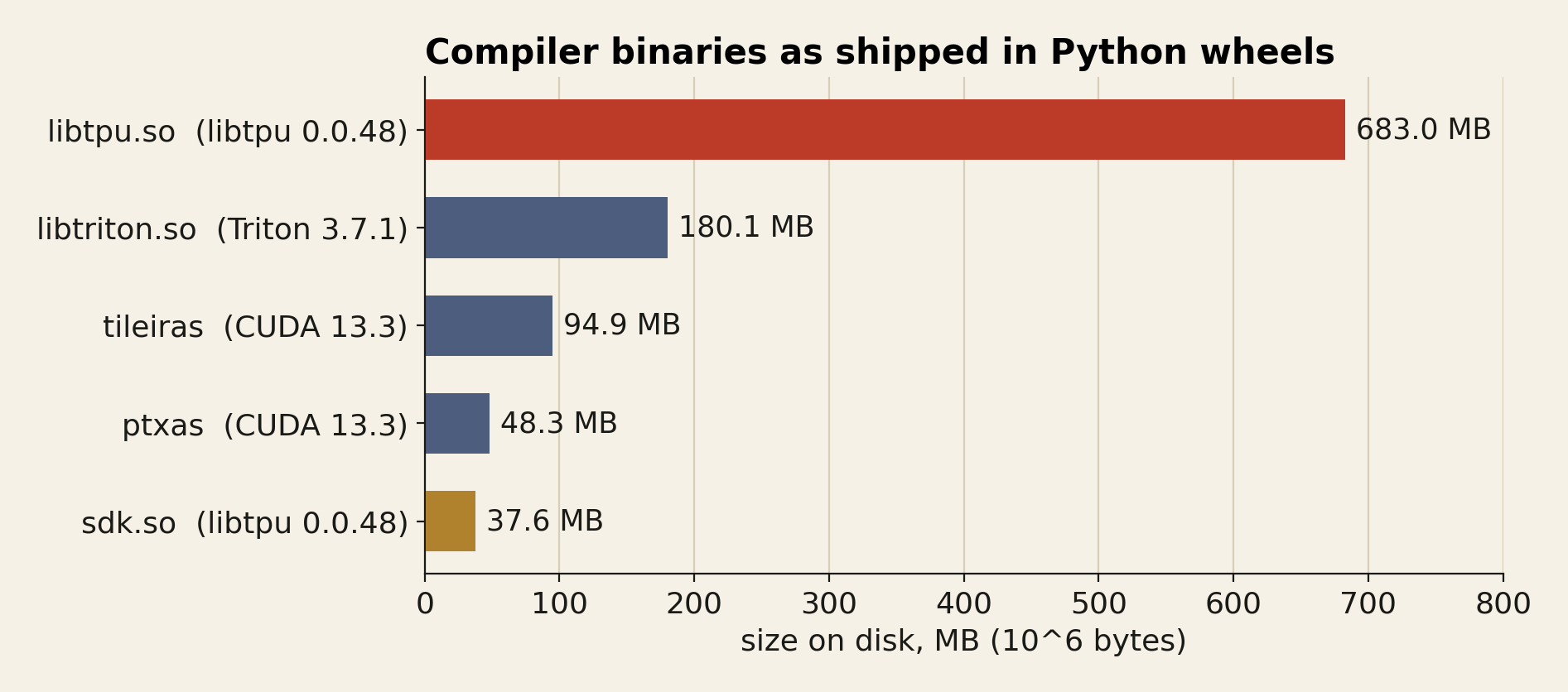
The size stops being surprising once you look at what is inside. ptxas is one stage of a pipeline. libtpu is the pipeline plus the runtime. Among its 4,237,056 printable strings, the token sparse_core appears 51,866 times, memory_space_assignment 3,100 times and mosaic, the Pallas back end, 828 times.
Source paths survive as strings: the TPU back end lives under platforms/xla/service/jellyfish, its debugger under platforms/deepsea/jellyfish/xdb.
The chips are numbered inside the binary. The protocol-buffer descriptor that defines the chip enum is embedded in the file, and decoding it gives TPU_VERSION_INVALID = 0, JELLYFISH = 1, DRAGONFISH = 2, PUFFERFISH = 3, VIPERFISH = 4, GHOSTLITE = 5 and 6acc60406 = 6, one value per family since TPU v2.
Ask the compiler which chip it is targeting and the target description it dumps answers: PUFFERFISH for a v4 compile, VIPERFISH for both v5e and v5p, GHOSTLITE for Trillium, and TPU_VERSION_6acc60406 for Ironwood. Every older family kept its codename in the shipped binary. The newest one ships as a string that looks like a hash.
A second enum, for core types, holds a small piece of history. It has TPU_CORE_TYPE_TENSOR_CORE = 1, TPU_CORE_TYPE_SPARSE_CORE = 3, and value 2 under two names: TPU_CORE_TYPE_BARNA_CORE and TPU_CORE_TYPE_SPARSE_CORE_V0. Google’s retrospective says the SparseCore was already on the TPU v2 die but was only disclosed in the TPU v4 paper. The binary still carries the first SparseCore’s other name, 7,570 times.
The option surface is just as large. The dump of the compilation environment lists 1,184 top-level options. 861 begin with xla_tpu_, 106 with xla_jf_, and 33 with xla_sc_ for the SparseCore.
Some read like a research agenda: the scheduler options include a biased random-key genetic algorithm with a generation limit that defaults to 1,200. Most will never matter to anyone outside Google. A handful decide things this piece is about, and we name them where they come up.
What the TPU compiler thinks each chip is
XLA keeps a roofline for every program it compiles. Each instruction gets a time equal to the larger of its FLOPs divided by a peak rate and its bytes divided by a bandwidth, and the sum is reported as optimal_seconds.
The rates are per-target constants, which means they can be read back. Compile a matmul large enough to be compute-bound and divide its FLOPs by its optimal_seconds. Compile an elementwise add large enough to be bandwidth-bound and do the same with its bytes.
We swept the matmul from 1,024 to 16,384 and the add from 64 MiB to 1 GiB, and both constants plateau exactly.
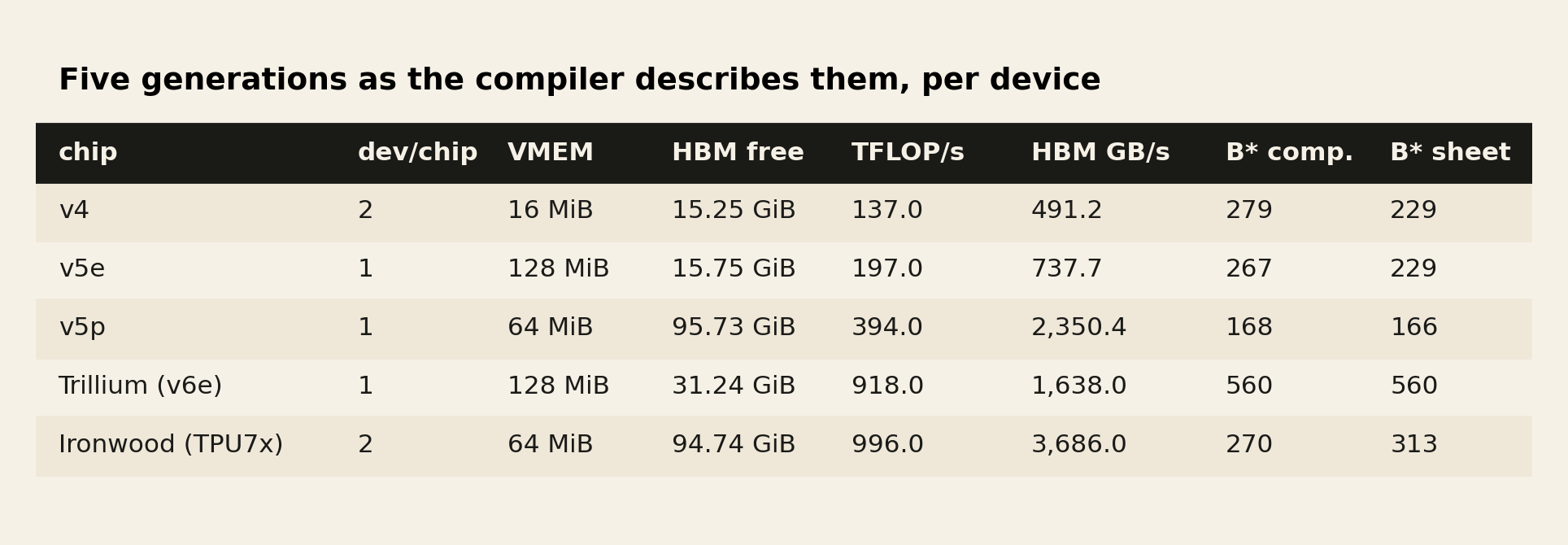
Two critical things in that table need explaining before anything else.
The first is the devices. In these topologies a v4 chip and an Ironwood chip each appear as two devices, with core_on_chip 0 and 1 at the same coordinates, while v5p appears as one device per chip because its two TensorCores are fused into one logical core called megacore.
Every training TPU since v2 has had two TensorCores that share only HBM, according to Google’s retrospective; megacore is a compiler illusion that started with v4. Ironwood drops it. Google’s TPU7x documentation says frameworks see each Ironwood chip as two devices, one per chiplet, a programming model closer to TPU v3 than to v4 or v5p.
Each Ironwood device has 94.74 GiB of HBM available, half of the chip’s 192 GiB minus a reserve, and 64 MiB of VMEM. Code written for v5p that assumed one device per chip sees twice as many on Ironwood, each with half the memory.
The second is the ratios between the compiler’s constants and Google’s published figures.
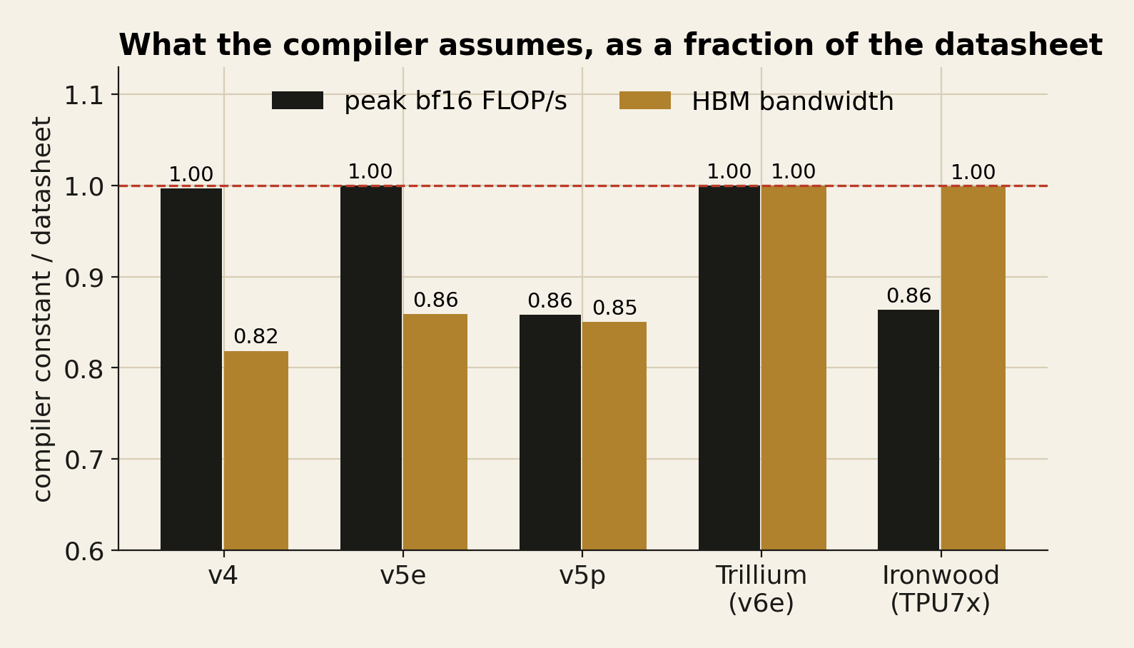
On Trillium the compiler’s constants are the datasheet: 918 TFLOP/s and 1,638 GB/s. On Ironwood its bandwidth is 3,686 GB/s per core, 7,372 per chip, within 0.11% of the 7,380 GB/s in Google’s documentation.
Google’s own sources don’t agree with each other here: the architects’ paper lists 7,300. Its compute is 996 TFLOP/s per core, 1,992 per chip, or 86.3% of the 2,307 Google lists. v5p carries the same kind of discount on both axes: 394 of 459 TFLOP/s and 2,350 of 2,765 GB/s, 85.8% and 85.0%. v5e and v4 match on compute and are discounted on bandwidth, to 85.9% and 81.9%.
One more cross-check falls out of the memory report: v5p’s 95.73 GiB of free HBM per device fits the 96 GiB in the retrospective better than the 95 GiB in the documentation table.
The binary doesn’t say whether the compute discounts are clock assumptions or margins, but it gives a hint. The low-level backend reports how many instructions of each kind fit in one bundle, and the MXU count changes between generations: four MXU slots per bundle on v4, v5e and v5p, two on Trillium and Ironwood.
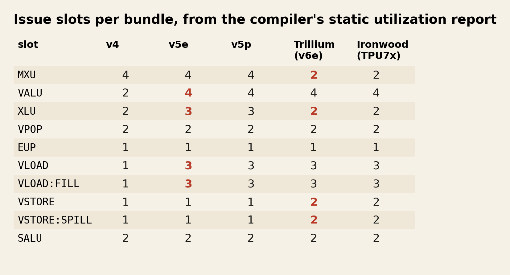
Divide the compiler’s cycle estimates for large matmuls by the number of MXU slots and you get the work one slot does per cycle. On the four-slot chips it is 15,350 to 15,860 bf16 multiply-adds, close to the 16,384 of one 128 by 128 systolic array.
That matches Google’s counts: four MXUs per TensorCore on v5e, eight 128 by 128 MXUs per chip on v4 and v5p. On Trillium a slot reaches 113,900 multiply-adds per cycle and on Ironwood 108,800, which is impossible for one 256 by 256 array (65,536) and consistent with two arrays per slot, or one array retiring two rows per cycle.
Combine slot rates with the published peaks and you get clocks the datasheets don’t print: 1.05 GHz for v4, which matches the 1,050 MHz in Google’s TPU v4 paper, 1.50 GHz for v5e, 1.75 GHz for v5p and Trillium, and 2.20 GHz for Ironwood. The retrospective describes Ironwood’s matrix units as four 256 by 256 arrays for bf16.
Counted per chip, reaching 2,307 TFLOP/s with four such arrays would need a 4.4 GHz clock; counted per TensorCore, it needs 2.2 GHz, which is what the compiler’s slot rates imply.
We read the paper’s four arrays as per TensorCore. Run the same arithmetic on the compiler’s constants instead of the datasheet and v5p drops to 1.50 GHz and Ironwood to 1.90 GHz.
One consistent reading is that the compiler models those two chips at a lower clock than their peak figures assume. Another is that it simply derates them. Either way, the compiler’s own roofline for Ironwood uses 996 TFLOP/s per core, not 1,153.
The critical decode batch, v4 to TPU 8i
In earlier pieces we kept coming back to one number: the decode batch at which a chip stops waiting for its weights. A decode step has to stream every weight from HBM at least once.
At small batch that stream is the whole cost, and adding sequences is nearly free until the arithmetic catches up. The crossover is B* = P·b / (2·B_hbm), where P is the FLOP rate at the precision you use, b the bytes per weight and B_hbm the bandwidth.
Because P usually doubles whenever b halves, B* barely moves with precision. On an H100 it is 295 whether you run bf16 or FP8, on a B200 about 281.
Between TPU generations it moves a lot.
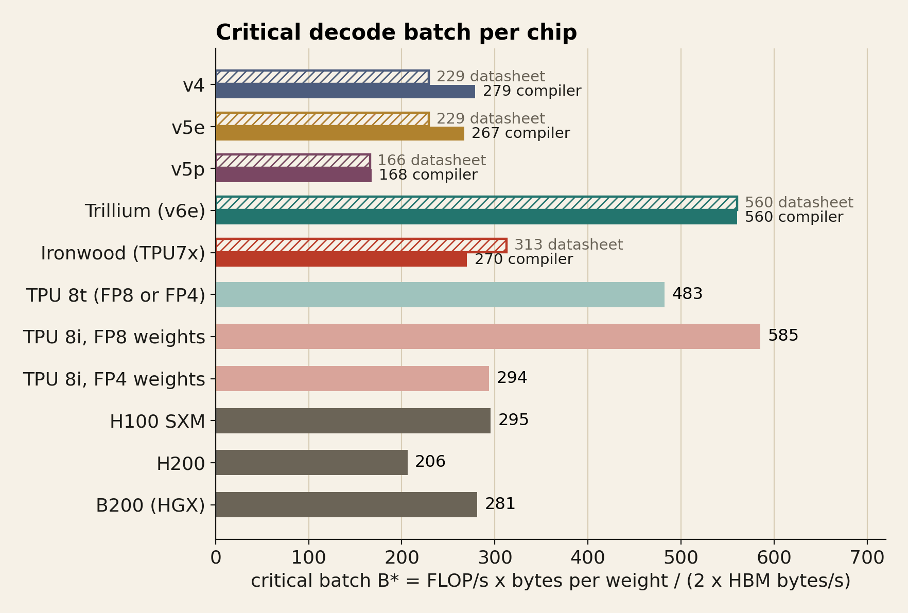
Trillium’s critical batch is 560, by the datasheet and by the compiler, which agree exactly. That is the highest of any shipping accelerator in this piece, NVIDIA’s included.
Trillium raised compute 4.7 times over v5e, and the slot table shows how: four times the multiply-adds per cycle, from half as many slots each eight times larger, at 1.75 GHz instead of 1.50. Bandwidth only grew 1.9 times, so Trillium needs about twice as many concurrent sequences per chip as an H100 before its FLOPs start to pay.
That’s an odd profile for a chip Google’s architects describe, in a footnote, as focused on inference. It suits batched, throughput-bound serving, and it punishes latency-bound decode.
Ironwood undid it. It raised bandwidth 4.5 times over Trillium, to 7,380 GB/s, while raising compute 2.5 times, which puts its critical batch at 313 on paper and 270 by the compiler’s constants, close to the H100’s 295 and the B200’s 281.
Google introduced Ironwood as its first TPU built for inference, and its architects list it as the fifth of their training supercomputers. In roofline terms both descriptions fit: it is the generation that brought the critical batch back down.
The compiler’s estimates agree when you compile real shapes. We compiled one 8192 by 28672 projection, the shape of a large dense MLP layer, at every batch from 2 to 2,048 and plotted the estimated time against batch 2.
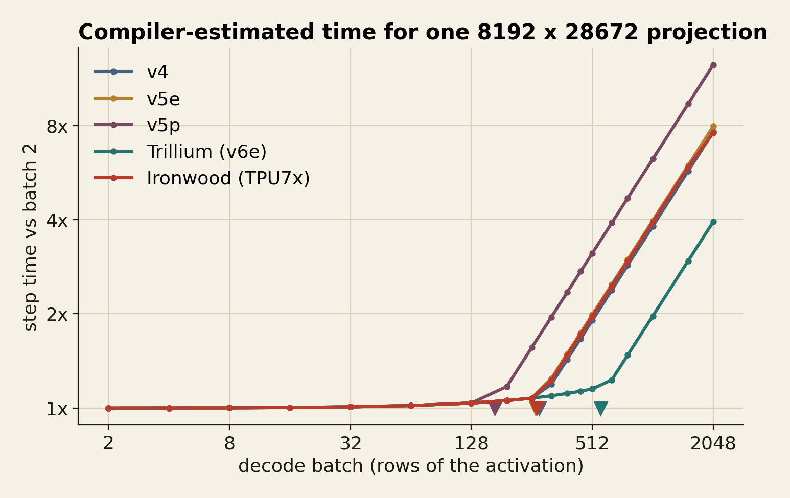
On Ironwood the estimate at batch 2 is 127.5 µs. It is 7.5% higher at batch 256 and 1.97 times higher at 512.
On Trillium it is 287 µs at batch 2, only 15.1% higher at batch 512 and 1.97 times higher at 1,024. v5p, the chip with the most bandwidth per FLOP, bends first: 17% above its floor at batch 192 and 56% above at 256. In absolute terms Ironwood is still the fastest at every batch, 251 µs at batch 512 against Trillium’s 330. What changes is where each chip stops being free.
The eighth generation splits the difference in an instructive way. TPU 8t keeps HBM bandwidth modest at 6,528 GB/s while doubling MXU throughput with native FP4, so its critical batch is about 482 at FP8 or FP4.
That’s a training chip. TPU 8i has more bandwidth, 8,601 GB/s, and by Google’s own numbers the same throughput at FP4 as at FP8: 10.1 PFLOP/s at FP4 per chip, and 11.6 EFLOP/s at FP8 across a 1,152-chip pod, which is 10.07 per chip. If those figures mean what they appear to mean, 8i’s critical batch is 585 with FP8 weights and 294 with FP4 weights.
That breaks the precision invariance our earlier pieces relied on, and it breaks it in a useful direction. On 8i, FP4 is not a way to get more FLOPs. It is a way to halve the bytes each decode step has to read, which halves the batch you need before the chip is busy.
It is a compute format on the training chip and a bandwidth format on the inference chip. One caveat: the per-chip FP8 rate comes from a pod total. If Google counts only the 1,024 active chips its Boardfly description mentions, FP8 would be 11.3 PFLOP/s per chip and the two formats would no longer match.
A batch of one
Below the critical batch every extra row is nearly free, so a batch of one should cost what a batch of eight costs. On Ironwood it does. On every older TPU, by the compiler’s own estimate, it costs about three times as much.
The reason is visible in the optimized HLO. Compile a [1, 8192] by [8192, 28672] product for v4, v5e, v5p or Trillium and there is no matrix multiply left in it. The compiler has rewritten the dot into an elementwise multiply followed by a reduction, which runs on the vector unit.
Give it two rows and you get a convolution, generated by the MXU emitter EmitAllBatchInSublanes. The rewrite comes from a pass whose source file name survives in the binary, tpu_dot_strength_reducer.cc, and it is controlled by the option xla_tpu_enable_dot_strength_reduction, which defaults to true.
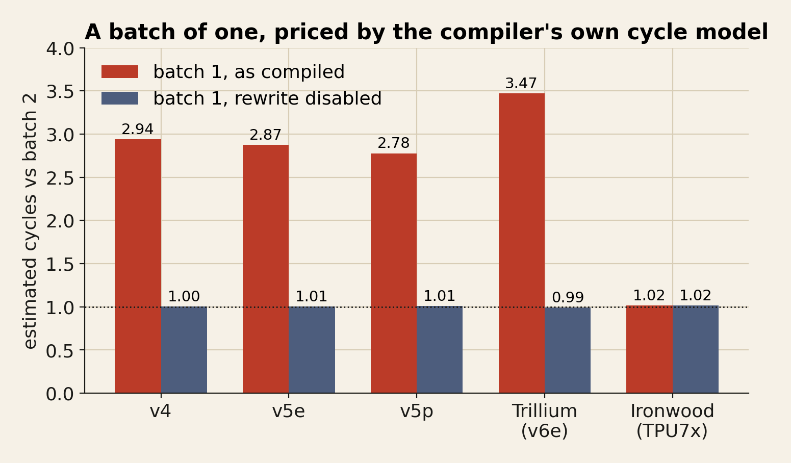
The cycle estimates attached to each program price the decision. On v4 the rewritten product takes 3,154,024 cycles against 1,077,235 on the MXU, 2.93 times as many.
On v5e it is 3,280,393 against 1,147,598 (2.86 times), on v5p 1,292,915 against 470,757 (2.75 times), and on Trillium 1,986,785 against 568,013 (3.50 times). Turn the option off with LIBTPU_INIT_ARGS=--xla_tpu_enable_dot_strength_reduction=false and batch one costs what batch two costs.
On Ironwood the pass doesn’t fire for this shape at all, and batch one stays on the MXU at 352,341 cycles either way.
The final bundles make the difference concrete. With the rewrite, Trillium’s program for a [1, 8192] by [8192, 1024] product contains no matrix instruction. It’s 855 vector multiplies, 506 vector adds, 966 unpack instructions that widen bf16 to f32, and 244 cross-lane broadcasts, permutes and rotates.
Without the rewrite, the same product is 128 matmul issues fed by 2,048 weight pushes, the same instruction stream the compiler emits for batch eight.
We don’t know why the rewrite is on. A plausible reason is that it was tuned for small matrices, where pushing weights into the MXU costs more than the arithmetic they feed. For an 8,192-wide projection the compiler’s cost model disagrees with its own pattern pass, and the pattern pass runs first.
In production this rarely bites, because serving engines usually pad the decode batch to a few fixed sizes so that each size compiles once, and the smallest size is usually larger than one. It does bite in hand-written single-stream decode loops, in draft models for speculative decoding that run at batch one, and in mixture-of-experts code that issues one dot per expert when an expert receives a single token.
If you run any of those on v5e or Trillium, the option is worth a test on real hardware. We can only tell you what the compiler predicts.
The tile and the KV cache
Every TPU array lives in tiles, and the layout string in the optimized HLO says which. A bf16 matrix is bf16[4096,4096]{1,0:T(8,128)(2,1)}: the last dimension varies fastest, the array is cut into tiles of 8 by 128 32-bit words, and (2,1) means two bf16 rows are packed into each word. f32 is T(8,128).
Eight-bit types are T(32,128)(4,1) and four-bit types T(64,128)(8,1). Every one of these tiles is 4 KiB. On the training chips from TPU v2 through v5p that is exactly one vector register, 8 sublanes by 128 lanes of 32 bits.
Ironwood’s registers are 16 by 256 according to the retrospective, four times larger, but its memory layouts use the same 8 by 128 tiles as every other generation we compiled for. Narrow types don’t get smaller tiles. They get more rows per word.
The compiler is careful with small arrays. For an array with one row it picks a T(1,128) tile instead of padding to eight rows, and for two or four rows T(2,128) or T(4,128).
What it can’t do is store less than one 32-bit word per lane. So on all five generations a single row of bf16 occupies twice its logical size, a single row of FP8 four times and a single row of FP4 eight times. FP4 activations need eight rows before they stop paying for air; FP8 needs four.
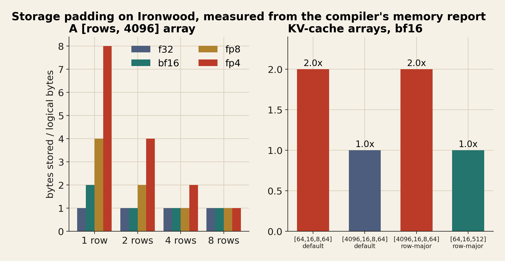
The minor dimension is less forgiving. Storage tiles are 128 elements wide on every generation, and a minor dimension narrower than that is padded unless the compiler can move a larger dimension into its place. When nobody constrains the layout, it does.
A [4096, 64] array is stored transposed, layout {0,1}, with the 4,096 dimension innermost, and costs exactly its logical size. A KV cache shaped [4096 pages, 16 tokens, 8 heads, 64 dims] gets layout {0,3,2,1}, with the page index innermost, and also costs exactly its size, as do the same cache with 16,384 pages, 16 heads or 32-token pages.
That default is a storage decision, not an access decision. It scatters each token’s 64-wide head across 64 sublane rows and interleaves 128 different pages in every vector, which is the opposite of what an attention kernel wants. Force the same cache into row-major order, layout {3,2,1,0}, and it costs 2.0 times its logical size, in bf16 and FP8 alike.
A small block such as [64, 16, 8, 64], which has no dimension of 128 or more to move inward, pays 2.0 times even in the default layout. Fold the heads into the minor dimension, [64, 16, 512], and row-major order pays nothing. With 128-wide heads the problem doesn’t exist.
Several open models use 64-wide heads, and on a TPU the layout of their KV cache decides whether half of it is padding. Kernels fix their own layouts, so this is a decision the kernel author makes once for everyone who uses the kernel.
This is the TPU version of a constraint we met on Blackwell, where the smallest UMMA tile has 64 rows. On NVIDIA the floor is in the math unit. On the TPU it is in the storage format, which means it costs HBM capacity and bandwidth, not just idle multipliers.
Precision: bf16, int8, FP8 and FP4 per generation
Datasheets list one number per format, when they list it at all. The compiler has to decide how to run every format on every chip, and its cycle estimates show what it decided.
We compiled one 8192 by 8192 by 8192 matmul in seven input types on all five generations and divided each estimate by the bf16 one.
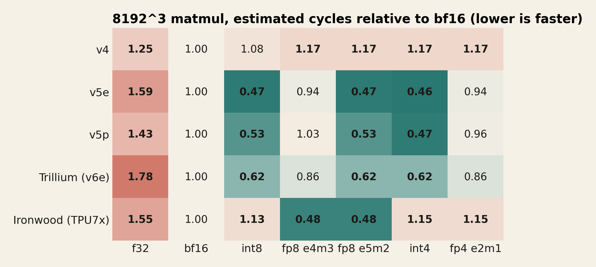
Ironwood runs FP8 in 0.48 times the cycles of bf16, which is the 2x Google advertises: 4,614 TFLOP/s against 2,307. It runs int8 in 1.13 times the cycles of bf16, slower than bf16, and int4 and FP4 in 1.15 times. Nothing in the optimized HLO converts the inputs. The emitter handles each narrow type itself, and on Ironwood only FP8 has a fast path in the cost model.
The older chips are the mirror image. int8 runs in 0.47 times the bf16 cycles on v5e, 0.53 on v5p and 0.62 on Trillium, consistent with the int8 rate Google publishes for v5e, 393 TOPS, twice its bf16 peak.
FP8 e4m3 gets little or nothing: 0.94, 1.03 and 0.86, in line with Google’s own table, which lists v5p and Trillium at the same FP8 rate as bf16. One result we can’t explain: FP8 e5m2 runs exactly as fast as int8 on v5e, v5p and Trillium, in the same number of cycles to the unit.
Either the cost model files e5m2 under the eight-bit integer path, or the hardware has a fast path for it that no datasheet mentions. Without a chip we can’t tell which. v4 accelerates nothing: every narrow type costs 1.08 to 1.17 times bf16.
Two practical consequences follow. If you serve int8-quantized weights on v5e or Trillium, those checkpoints lose their speed on Ironwood and should be re-quantized to FP8 before the migration, not after. And no chip the public compiler knows runs FP4 faster than its eight-bit path.
TPU 8t is the first TPU with native FP4, and on 8i, as above, FP4 appears to run at the FP8 rate. Our FP4 piece compared NVIDIA’s NVFP4 with the OCP MXFP4 format that AMD uses. Google hasn’t said, in the material we read, which FP4 the eighth generation uses or how it scales its blocks.
Inside one matmul on Trillium and Ironwood
The deepest thing libtpu will show you is its low-level IR, which it calls LLO, all the way to the final bundles. For a single 1024 by 1024 by 1024 bf16 matmul, the two dump options write 72 stages for Ironwood and 73 for Trillium.
The names read like a compiler textbook written for a VLIW machine: pre-auto-mxu-assigner, bf16-coalescing, x8-coalescing, MXU-assigner, vmac-transform, critical-path-scheduler, vliw-packed-bundles, vliw-bundle-scheduler, register-pressure, post-ra, delay-converter and, last, final_bundles. Trillium has one stage Ironwood doesn’t, post-allocation-offset-shuffling.
A bundle is the set of instructions issued together. TPU v2’s scalar unit fetched bundles of 322 bits, according to the retrospective, and Ironwood’s are more than 50% wider.
The slot table above says what one can hold. On both Trillium and Ironwood it is two MXU instructions, four vector ALU operations, two cross-lane operations, two result pops, one transcendental, three vector loads, two vector stores and two scalar operations, plus dedicated slots for spill traffic.
At the level of the instruction format the two TensorCores are identical. The programs they get are not.
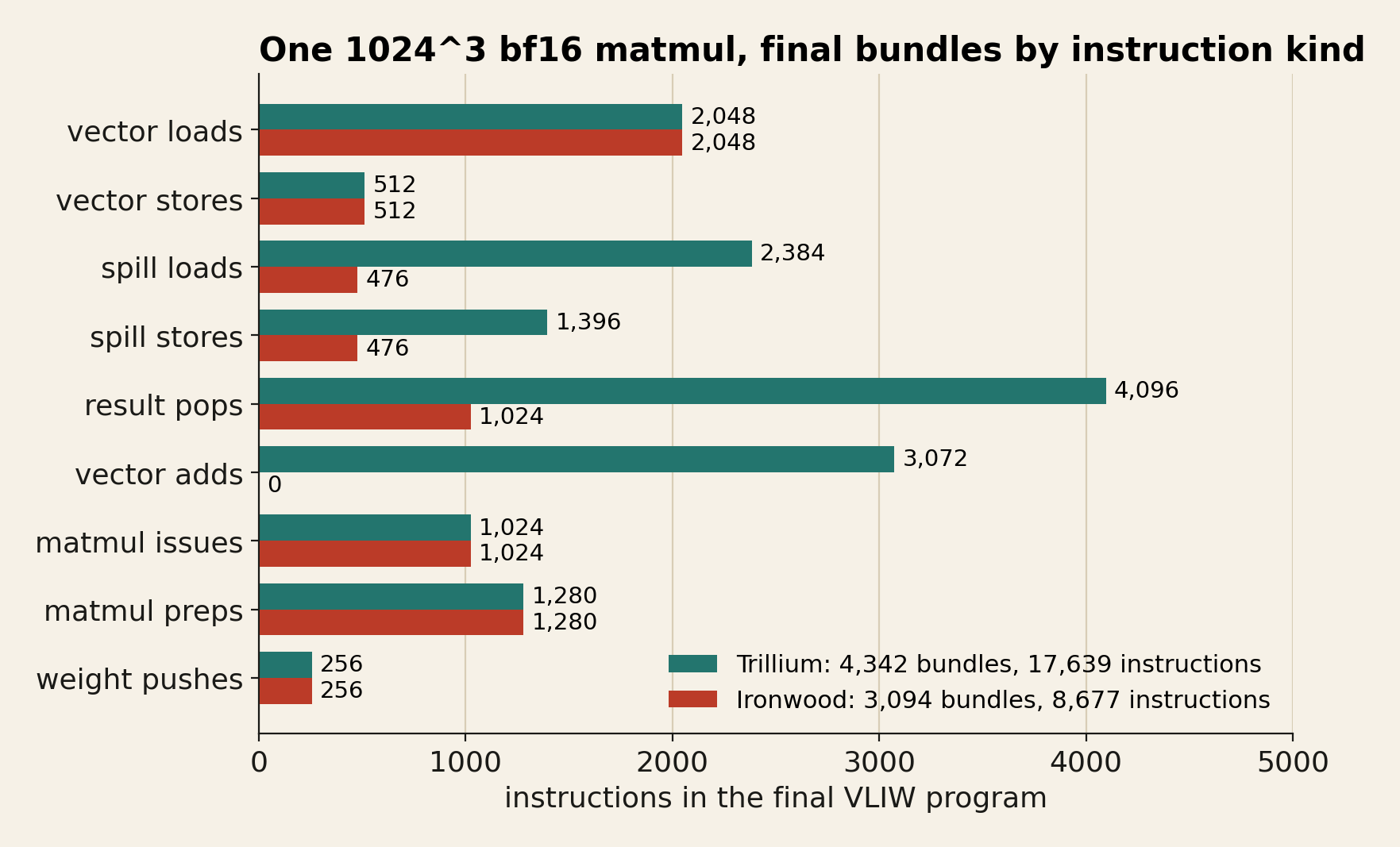
Trillium’s program is 4,342 bundles and 17,639 instructions. Ironwood’s is 3,094 bundles and 8,677 instructions. Strip out the spills and both load the same 2,048 vectors and store the same 512 results, and both issue the same 1,024 matrix multiplies after the same 256 weight pushes.
Everything else is the cost of getting partial sums out of the matrix unit. Trillium pops 4,096 results and Ironwood 1,024. Trillium executes 3,072 vector adds and Ironwood none. Trillium issues 2,384 spill loads and 1,396 spill stores, Ironwood 476 of each.
Here are three consecutive bundles from the middle of Trillium’s program, with registers renamed and VMEM addresses shortened:
vmatmul.mubr.bf16.gmra.mxu0 v51 ;; v21 = vpop.f32.mrf.mxu0 ;; vmatprep.mubr.bf16.mxu1 v61 ;; v30 = vld [buf+0xc30]
vmatprep.mubr.bf16.mxu0 v44 ;; v24 = vpack.c.bf16 v41, v23 ;; v3 = vadd.f32 v19, v5 ;; v57 = vadd.f32 v21, v22
    ;; v1 = vpop.f32.mrf.mxu1 ;; vmatpush1.bf16.msra.mxu1 v45 ;; v41 = vld [spill] ;; v23 = vld [spill] ;; v21 = vld [spill]
v31 = vpop.f32.mrf.mxu0 ;; v45 = vld [spill] ;; v22 = vld [spill]
and four from Ironwood’s:
v21 = vpop.f32.mrb[225].mxu0 ;; v43 = vpack.c.bf16 v37, v19 ;; v0 = vpop.f32.mrb[226].mxu1
v27 = vpack.c.bf16 v21, v62 ;; v12 = vpop.f32.mrb[226].mxu0 ;; v40 = vpop.f32.mrb[227].mxu1 ;; v21 = vld [spill]
v33 = vpop.f32.mrb[227].mxu0 ;; vst [buf+0xe08] v43 ;; v41 = vpack.c.bf16 v40, v0
vst [buf+0xe00] v27 ;; v63 = vpack.c.bf16 v33, v12 ;; vmatmul.mubr.bf16.gmra.mrb[76].mxu1 v2 ;; v27 = vld [spill]
On Trillium, results leave the matrix unit through something called mrf, with no address, and are added together on the vector unit while partial sums wait in registers and spill to VMEM. On Ironwood the matrix instruction names a destination, mrb[76], and each pop names a source, mrb[225], and nothing is added afterwards. Across the whole program the indices run from mrb[0] to mrb[255].
The counts fit one reading exactly. The 1024 by 1024 f32 output is 1,024 vector registers’ worth of 8 by 128 tiles. Trillium pops each of them four times, because one 256-deep pass through the matrix unit covers a quarter of K = 1024, and sums the four partials with three adds: 4,096 pops and 3,072 adds. Ironwood pops each one once.
A decode-shaped product, [8, 8192] by [8192, 1024], has 8 output tiles and a K that takes 32 passes. Trillium pops 256 times and adds 248 times; Ironwood pops 8 times and adds nothing.
We read mrf as matrix result FIFO and mrb as matrix result buffer: on Ironwood, partial sums accumulate inside the matrix unit, in addressed entries, for as many passes as K needs. That interpretation is ours, not Google’s. It is the same move NVIDIA made between Hopper and Blackwell, when the tensor core’s accumulator left the register file for tensor memory.
In our TMEM piece the reason was that Blackwell’s largest accumulator no longer fit in 255 registers. Here the measurable effect is that the vector unit stops doing the matrix unit’s bookkeeping. The result-pop slots are busy 16.5% of the time on Ironwood against 47.2% on Trillium, the vector ALUs 12.4% against 26.5%, and the spill-store slots 7.7% against 16.1%, while the MXU slots stay above 90% on both.
Those idle slots now have a second use. The retrospective describes a hardware replay unit in Ironwood’s vector unit that samples vector bundles at random and re-executes them in idle VLIW slots, replaying odd-lane operations on even lanes to catch silent data corruption without slowing the program. A matmul that leaves seven in eight vector ALU slots empty gives it plenty of room.
A caution about where the accumulator matters. In the decode-shaped program both chips spend about 4,100 bundles, dominated by roughly 8,200 vector loads and 2,048 weight pushes. When a program is a stream of weights, an accumulator saves little.
It matters for prefill, for training and for any matmul deep enough in K that partial sums pile up, which is exactly the work that turns into spills on Trillium.
SparseCores, collectives and MoE dispatch
SparseCores are small dataflow processors built for embedding lookups. Google’s retrospective counts two per chip on TPU v2 and v3 and four on v4, v5p and Ironwood; Google’s documentation gives Trillium two. Each has 16 compute tiles; together they take about 5% of the die area and of the power, and Ironwood’s are 2.4 times faster than v5p’s.
The retrospective also says they began serving as offload engines for collectives such as AllReduce, AllGather, ReduceScatter and Broadcast once Transformers took over the workload. In the public compiler, with default options, that only happens on Ironwood.
Compile an all-reduce across four Ironwood chips, eight devices, and the optimized HLO contains no all-reduce running on the TensorCore.
It contains an asynchronous call on an execution thread named sparsecore, with a configuration that says "device_type":"DEVICE_TYPE_SPARSECORE" and "offload":"OFFLOAD_COLLECTIVE", and a ring description in which one phase is marked "across_cores_on_chip":true, the hop between the two TensorCores of a chip. The TensorCore starts the call and carries on. The SparseCores move the data.
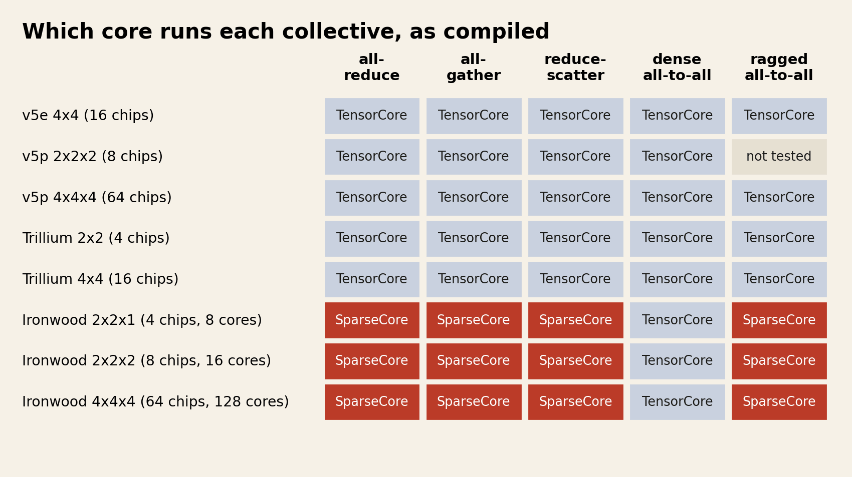
We compiled all-reduce, all-gather, reduce-scatter and the dense all-to-all at 64 KiB, 1 MiB and 16 MiB per device on Ironwood slices of 4, 8 and 64 chips and on v5e, v5p and Trillium slices, plus the ragged all-to-all that JAX uses for mixture-of-experts dispatch.
On Ironwood, all-reduce, all-gather and reduce-scatter were offloaded to the SparseCores in every case that compiled, and so was the ragged all-to-all, on 8, 16 and 128 devices. The dense all-to-all never was, on any generation. On v5e, v5p and Trillium nothing was offloaded, although v5p has four SparseCores per chip.
Their collectives run on the TensorCore, with a short-message all-reduce emitter and a ring emitter above it; on the 2- to 4-device slices we bisected, the switch happens just under 1 MiB per device, and around 2 MiB on v5p. A two-device collective on Ironwood, whether between the two cores of one chip or between neighboring chips, also stays on the TensorCore.
The library behind these choices is large. libtpu’s strings name 146 distinct identifiers ending in Emitter or Strategy, among them a D2DUniDirRingStrategy for the die-to-die hop inside a chip, an InferenceShortRingSumEmitter, a RaggedAllToAllEmitter and a RotatedPincerQuantizedEmitter, whose name suggests collectives on quantized data. Our compiles used a handful of them, and each choice is recorded in the HLO.
The switches are in the compilation environment. xla_tpu_enable_sparse_core_collective_offload_all_reduce, _all_gather and _reduce_scatter are set to AUTO, and xla_tpu_sparse_core_all_reduce_offload_min_size_in_bytes is 65,536, so very small all-reduces stay where they are.
Read that next to Google’s description of TPU 8i. Each 8i chip has two TensorCores on core dies and one Collectives Acceleration Engine on the chiplet die, “replacing four SparseCores” of Ironwood, with five times lower on-chip collective latency, plus a new topology, Boardfly, that cuts the worst path across a 1,024-chip pod from 16 hops to 7 to speed up all-to-all traffic.
On Ironwood the SparseCores are already the TPU’s collectives engine, MoE dispatch included. TPU 8i replaces them with hardware built only for that job and attacks the remaining cost, hop count, through the network. TPU 8t keeps its SparseCores, and Google describes them as offloading data-dependent all-gathers and other collectives too.
For serving, the reason to care is tensor parallelism. A Megatron-style transformer layer performs two all-reduces per layer in decode, each of batch times hidden times two bytes: 1 MiB at batch 64 and a hidden size of 8,192, right where the older chips switch emitters.
On Ironwood that traffic, and the MoE dispatch next to it, leaves the TensorCore, which can keep multiplying while it moves.
VMEM and TPU 8i’s 384 MB
VMEM is the TPU’s software-managed on-chip memory, where a Pallas kernel stages its tiles. The compiler enforces its size and says so when you ask for too much.
We compiled a Pallas kernel with an ever larger scratch buffer until it failed, which on Ironwood reads “Allocation (size=68157440) would exceed memory (size=67108864)”. The limits per device: v4 16 MiB, v5e 128 MiB, v5p 64 MiB, Trillium 128 MiB, Ironwood 64 MiB per core.
Per chip that is 32 MiB on v4 and 128 MiB on v5e, v5p, Trillium and Ironwood, which matches the retrospective’s table for the training chips; on v5p a megacore program is still limited to one core’s 64 MiB.
XLA’s own fusions stay well below that: on Ironwood the large matmul fusions carried a 32 MiB scoped budget, and the largest fusion allocations we saw were about 15 MB on v4, v5e and v5p and up to 33 MB on Trillium and Ironwood. A kernel that wants the rest has to ask for it.
The same trick gives HBM. Compile something larger than memory and the error reports the space available per device: 15.25 GiB on v4, 15.75 on v5e, 95.73 on v5p, 31.24 on Trillium and 94.74 per Ironwood core.
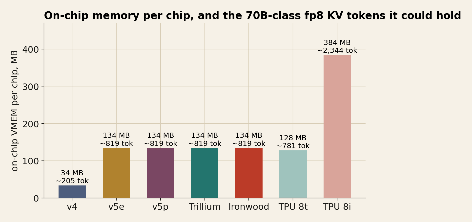
On-chip memory per chip has been 128 MiB on every TPU since v5e and v5p. The retrospective’s explanation is that SRAM density grew more slowly than logic density, so VMEM only quadrupled from TPU v2 to Ironwood while the die grew much more.
TPU 8i is the first chip in this lineage to break the plateau, with 384 MB of on-chip SRAM, three times Ironwood, and Google says it can host a larger KV cache entirely on silicon. It is worth putting a number on larger.
A 70B-class model with grouped-query attention, 80 layers and 8 KV heads of 128, stores 163,840 bytes of KV per token in FP8. 384 MB holds about 2,300 of those tokens, and only if nothing else lived in VMEM. Ironwood’s 128 MiB holds about 820. A model with DeepSeek’s compressed latent attention, 576 values per token per layer over 61 layers, needs 35,136 bytes per token, so 8i holds about 10,900 tokens of it.
Per chip that is one modest conversation. Per pod it is another matter: 1,152 chips carry 442 GB of SRAM, about 2.7 million tokens of the 70B-class cache. On-chip KV is a pod-scale idea.
It works when the cache is sharded across hundreds of chips that can reach each other quickly, which is what the collectives engine and Boardfly are for. The SRAM, the CAE and the topology only make sense together.
The bill: TPU vs GPU, per byte and per FLOP
As of September, Google’s pricing page lists Ironwood at $12.00 per chip-hour on demand in Iowa, $8.40 on a one-year commitment and $5.40 on three years.
Trillium lists at $2.70 on demand and $1.22 on three years, v5p at $4.20 and $1.89, v5e at $1.20 and $0.54. SemiAnalysis estimates that Anthropic pays about $1.60 per Ironwood chip-hour on Google Cloud. For GPUs on the same cloud, a September snapshot of public prices put an H100 at $5.38 and a B200 at $11.28 per GPU-hour on demand.
The transacted neocloud market, as measured by Ornn’s index on 28 September, was $2.56 for an H100 and $8.11 for a B200.
Every hourly rate hides two prices. One is what you pay per unit of HBM bandwidth, which is what a decode step below the critical batch consumes. The other is what you pay per unit of compute, which is what you consume above it.
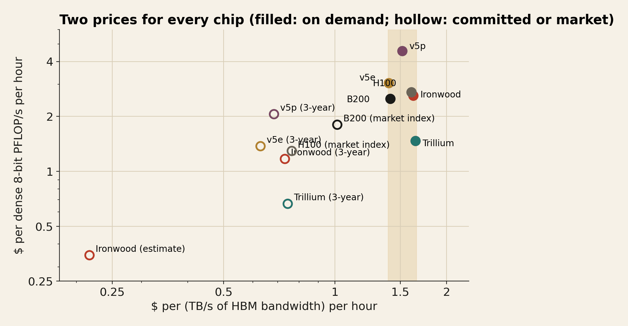
On demand, the first price is almost the same for all six accelerators we priced: $1.40 per TB/s-hour for v5e, $1.41 for the B200, $1.52 for v5p, $1.61 for the H100, $1.63 for Ironwood and $1.65 for Trillium.
The second ranges more than threefold, from $1.47 per dense 8-bit PFLOP/s-hour on Trillium to $4.58 on v5p. Whether by design or by convergence, Google’s on-demand rate card prices bandwidth and lets FLOPs fall where they may.
That has a direct consequence for tokens. Take a 70B-class dense model with 8-bit weights and short contexts, and assume a perfect roofline: no KV traffic, no communication, no idle time, and per-chip throughput that doesn’t depend on how many chips the model is split across. These are floors, not forecasts.
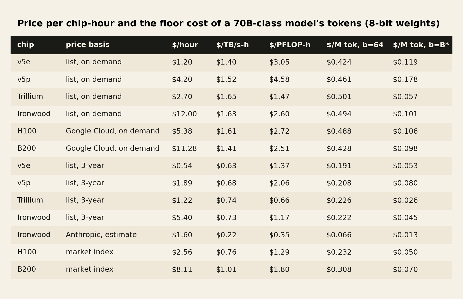
At batch 64 every chip in the table is bandwidth-bound, and the on-demand floor per million output tokens lands between $0.42 and $0.50 on all of them. The chip doesn’t matter, because the rate card has already priced the bandwidth.
At each chip’s critical batch the floor falls to between $0.057 on Trillium and $0.18 on v5p, and now the chip matters a great deal. Trillium is the cheapest FLOP Google sells, as long as you can keep 560 sequences per chip in flight.
Ironwood’s floor at its critical batch is $0.10 on demand, $0.045 on a three-year commitment, and $0.013 at the estimated Anthropic rate, about a quarter of the transacted H100 market’s $0.050 and a fifth of the B200’s $0.070.
Long contexts push every chip back toward the bandwidth price, whatever the batch. With an FP8 KV cache, the same model reads 163,840 bytes per token for every position of context, so at 32K tokens each generated token reads 5.4 GB of cache no matter how many sequences share the weights.
That caps utilization at 4.2% of peak on Ironwood, 2.3% on Trillium, 4.4% on an H100 and 4.6% on a B200, and it puts the on-demand floor at between $2.08 and $2.46 per million output tokens on every chip in the table, about five times the short-context floor at batch 64.
For agentic workloads with long contexts, the rate card’s bandwidth price is the price of a token, which is why so much attention research in the last year has been about reading fewer bytes of cache.
The comparison at the critical batch is the economic story of the TPU in 2026. At list price Ironwood is priced like a B200 on Google Cloud, $12.00 against $11.28, and the same rate card puts every chip near the same bandwidth price.
At the price a tenant with a gigawatt-scale contract reportedly pays, Ironwood is the cheapest accelerator in this piece on both axes, by 1.9 to 2.9 times over the next cheapest option. The scale of those contracts is public now. Broadcom booked $10 billion and then another $11 billion of Ironwood racks for Anthropic, describing them as complete system sales, and in September put Anthropic’s deployment at 1 GW of Ironwood in 2026, 5 GW of TPU 8i in 2027 and 10 GW in 2028.
Meta signed a multi-year TPU rental in February and is negotiating to buy chips for its own data centers from 2027.
Tenants also change what the compiler is. A chip that only Google ran could keep its codenames, its 1,184 options and its rewrites to itself. A chip rented by Anthropic and Meta has customers who will read the same dumps we read, find the same options and tune them. For now, the most detailed description of the TPU’s internals that anyone outside Google can read is a 683 MB binary.
Economic and financial implications
Everything above is a property of a chip or of a compiler. Money turns those properties into decisions, and in 2026 the decisions are large enough to show up in the earnings of three companies. Start with what the findings are worth to a buyer, then follow the money up the stack.
What the compiler’s findings are worth to a buyer
Four results in this piece change the cost of a token directly, using the same floor model as the table above.
Precision on Ironwood. The compiler prices an int8 matmul at 1.13 times the bf16 cycles and an FP8 matmul at 0.48 times. Above the critical batch, where compute sets the price, an int8 checkpoint costs about 2.3 times as much per token as the same model in FP8. Below it, both read one byte per weight and cost the same. The penalty lands on the high-batch traffic that pays for a deployment.
The KV layout. At 32K tokens of context the cache dominates every byte a decode step reads. For a model with 64-wide heads and the same cache size per token as our reference model, a row-major cache stores and moves twice its logical size, which doubles the long-context floor, from $2.08 to $2.46 per million output tokens on demand to $4.17 to $4.92.
Batch one. For single-stream decode on v4 through Trillium, the multiply-and-reduce rewrite costs 2.75 to 3.50 times the cycles of the matrix-unit path in the compiler’s model. A latency-bound product that runs one sequence per replica pays that multiple on every token, unless someone changes one option.
Which generation. At three-year list prices Trillium’s dense 8-bit compute costs $0.66 per PFLOP/s-hour, the cheapest in this piece, and its bandwidth $0.74 per TB/s-hour, the same as Ironwood’s $0.73. Above 560 concurrent sequences per chip Trillium’s floor is $0.026 per million tokens against Ironwood’s $0.045.
Below that, the two cost the same per byte. Offline work that can keep hundreds of sequences in flight, such as evaluations, synthetic data and reinforcement-learning rollouts, is Trillium’s economic home. Interactive serving is Ironwood’s.
The rate card is a formula
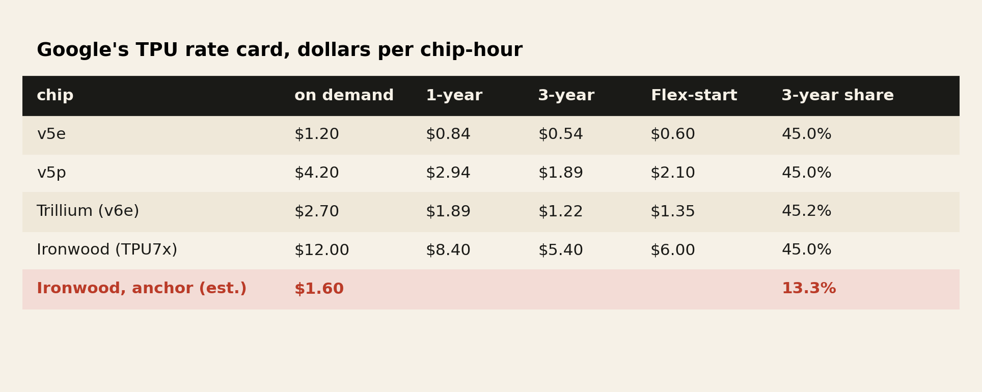
Google’s TPU prices follow a fixed schedule. For every generation with a published price, the one-year commitment is 70% of the on-demand rate, the three-year commitment 45% and Flex-start 50%: $0.84, $0.54 and $0.60 against $1.20 for v5e; $2.94, $1.89 and $2.10 against $4.20 for v5p; $1.89, $1.22 and $1.35 against $2.70 for Trillium; $8.40, $5.40 and $6.00 against $12.00 for Ironwood.
The estimated rate for Anthropic, $1.60 per Ironwood chip-hour, is 13.3% of on-demand. It is not on the card, and it is a different kind of price: a tenant price for gigawatts rather than a list price for hours.
What a gigawatt costs and earns
Broadcom booked $21 billion of Ironwood racks for Anthropic and describes Anthropic’s 2026 deployment as 1 GW of Ironwood: roughly $21 billion of rack hardware per gigawatt, before buildings, power and the network outside the racks.
On the revenue side, one Ironwood chip rented for 90% of the hours in a year earns $12,600 at the estimated anchor rate, $42,600 at the three-year list rate, $66,200 at the one-year rate and $94,600 on demand.
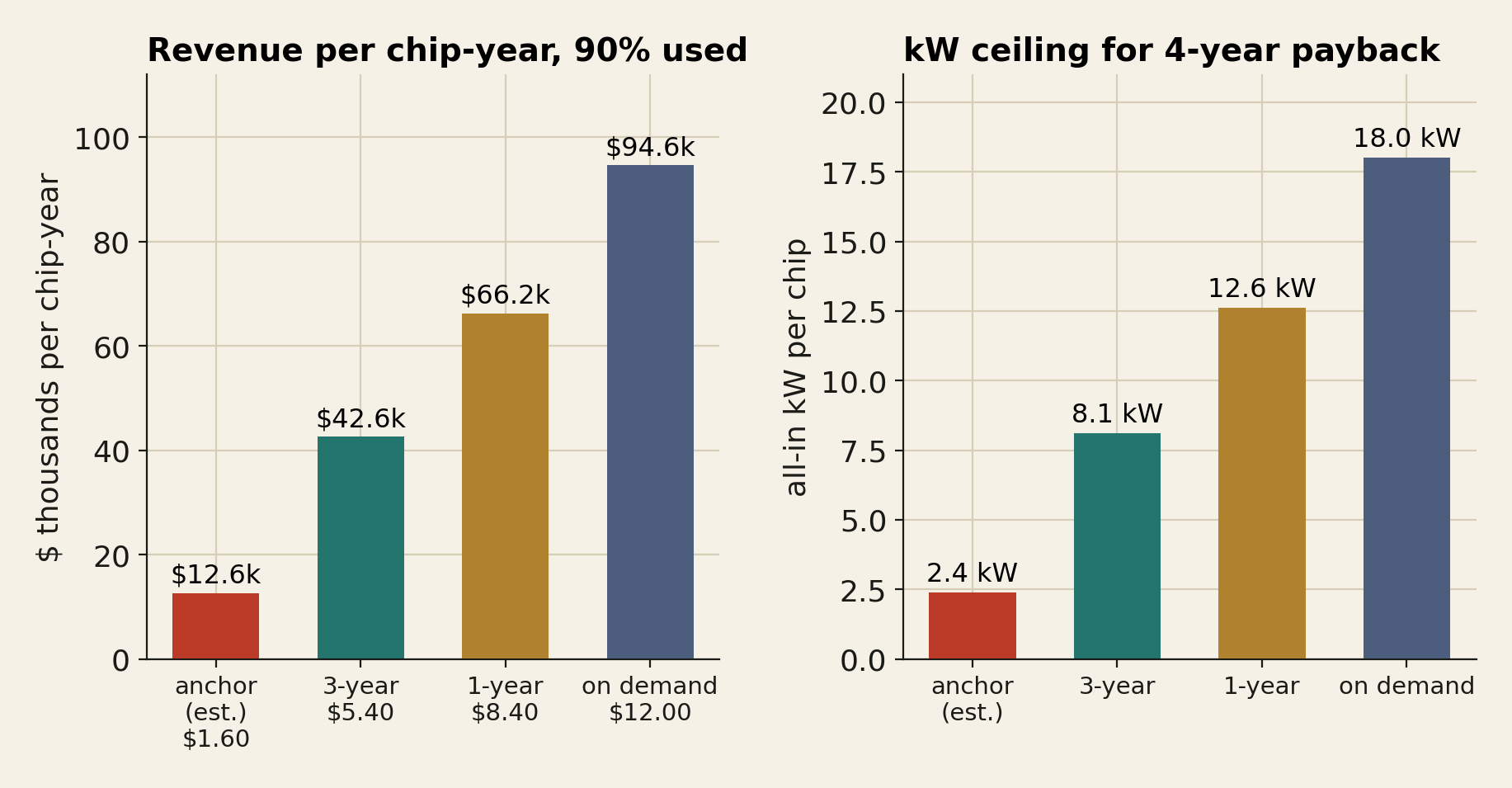
Google doesn’t publish Ironwood’s power per chip, so the two numbers can’t be joined directly. They can be joined conditionally. For the anchor rate to repay $21 billion of racks in four years at 90% utilization, a gigawatt has to hold about 416,000 chips, which means each chip, with its share of host, network and cooling, can draw no more than about 2.4 kW.
At the three-year list rate the same payback allows 8.1 kW per chip, and on demand 18 kW. At any published price the racks pay for themselves in well under four years. At the anchor price the answer depends on watts per chip, a number Google hasn’t published. Energy and buildings come on top of all of these.
Who captures the margin
A GPU buyer pays NVIDIA’s gross margin: 75.0% in the quarter to July, guided to 74.0% for the next and, according to the company’s call, heading for a trough of 71% to 72% in its fiscal fourth quarter as memory costs rise.
A TPU buyer pays Google, which pays Broadcom, whose company-wide gross margin was also 75% in its quarter to August but fell 210 basis points in a single quarter because AI chips, 73% of them custom accelerators, made up more of its revenue.
The gap between those two margin stacks is the room Google has to price anchor tenants far below its own list. It is also how the B200 rental index could rise 79% in a quarter while Ironwood capacity went to Anthropic, by SemiAnalysis’s estimate, at about a fifth of the B200’s market rate.
Alphabet
Alphabet’s filings now describe the TPU as something it sells. Its first-quarter 10-Q says Google Cloud has agreements to supply multiple gigawatts of TPU hardware to customers who run their own infrastructure, with the revenue counted in the Cloud backlog.
That backlog reached $514 billion at the end of June, up more than $50 billion in a quarter. Google Cloud revenue grew 82% to $24.8 billion in the second quarter, with a 35.6% operating margin, and management said growth accelerated even after excluding TPU system sales.
The bill is on the other side of the ledger. Alphabet raised its 2026 capital-expenditure guidance to $195 billion to $205 billion, spent $44.9 billion in the second quarter alone and reported negative free cash flow of $5.9 billion for the quarter.
On 1 June it announced up to $70 billion of new equity: $15 billion of mandatory convertible preferred stock, $15 billion of common stock and a $40 billion at-the-market program, to fund AI infrastructure. It has also reportedly agreed a joint venture with a large investment firm to lease TPUs to other customers.
A company that funds part of its build-out with equity has to care about the utilization and the price of every chip, which is the trade-off an 87% discount to list makes visible.
Broadcom
Broadcom’s AI semiconductor revenue was $16.7 billion in its quarter to August, up 221% and 56% of total revenue, with custom accelerators 73% of it.
It shipped Ironwood in high volume to Anthropic and to Google, began production shipments of TPU 8i for Google, and guided AI revenue to $58 billion for fiscal 2026, $115 billion for fiscal 2027 and $230 billion for fiscal 2028. On the same call it gave Anthropic’s roadmap: 1 GW of Ironwood in 2026, 5 GW of TPU 8i in 2027 and 10 GW in 2028.
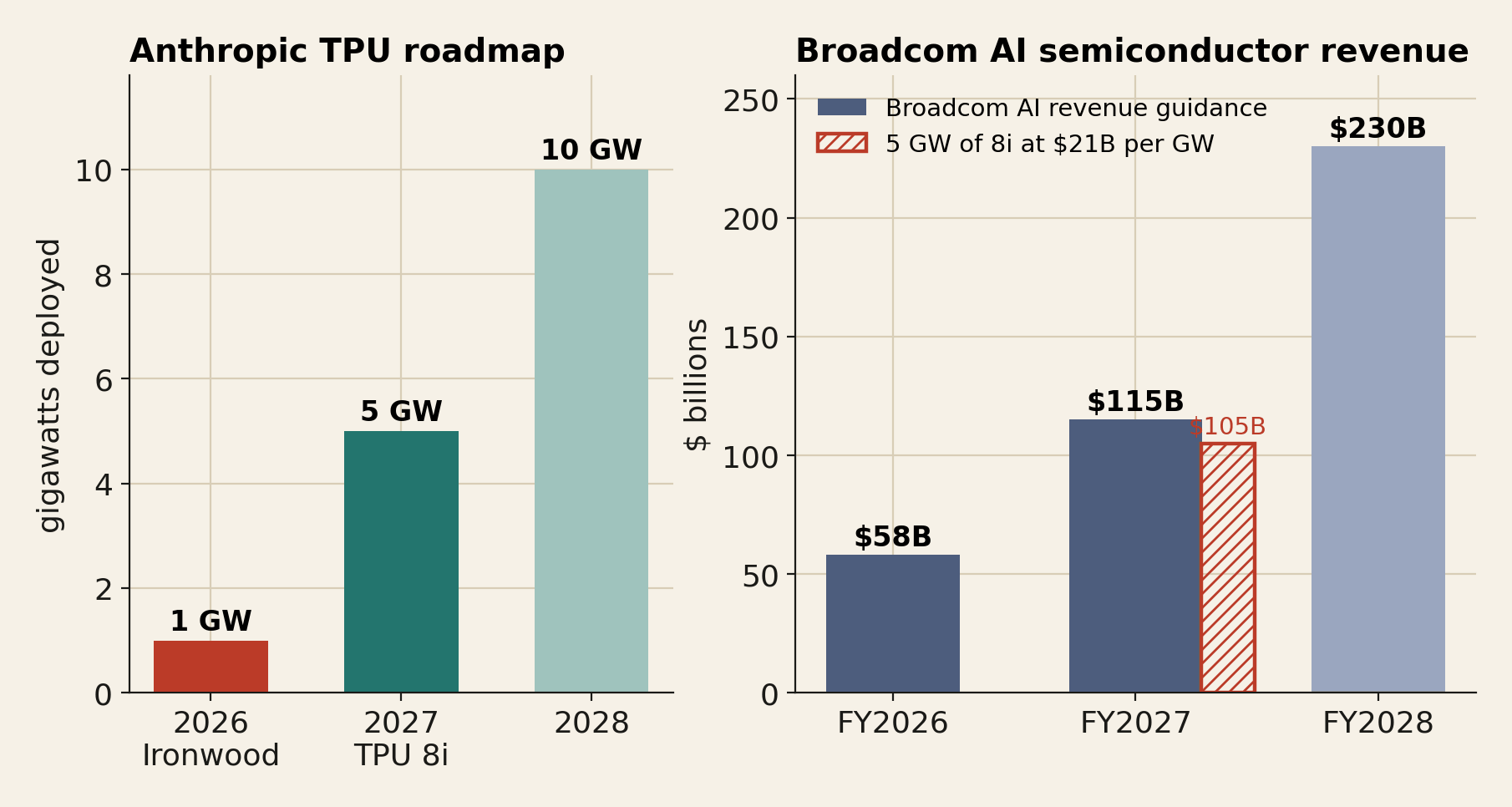
Put the two together and something has to give. If TPU 8i racks cost what Ironwood racks cost per gigawatt, Anthropic’s 2027 deployment alone would be about $105 billion of hardware, close to Broadcom’s entire $115 billion fiscal-2027 AI guidance, which also has to cover Google’s own TPUs, other custom-chip customers and networking.
Either TPU 8i is much cheaper per gigawatt than Ironwood, or a large share of the value flows through Google’s TPU system sales rather than through Broadcom’s revenue, or both.
Reports conflict on which partner designs which eighth-generation chip, and Google hasn’t confirmed any of them; Broadcom’s own call places TPU 8i in its shipments.
MediaTek and the inputs
MediaTek is Google’s second TPU partner. It reportedly holds orders for Google’s v7e and v8e, asked TSMC for a sevenfold increase in CoWoS packaging capacity for its Google projects by 2027, and expects more than $1 billion of ASIC revenue in 2026 and several billion in 2027.
Digitimes reports that its TPU orders are now limited by capacity. The binding inputs for every TPU, as for every GPU, are advanced packaging and HBM. NVIDIA attributes its margin step-down to memory costs, and each new TPU carries more HBM than the last: 192 GiB on Ironwood, 216 GB on TPU 8t and 288 GB on TPU 8i.
A rate card that is flat in dollars per unit of bandwidth is consistent with HBM being the input that sets the cost.
Nvidia
NVIDIA’s own numbers show no damage yet: revenue of $96.2 billion in the quarter to July, up 106%, data-center revenue of $89.0 billion, guidance of $108 billion for the next quarter and about 70% growth for fiscal 2028.
Demand still exceeds supply. What TPUs change is the price at the margin. The largest buyers outside Google now have a second supplier: Anthropic is scaling toward 10 GW of TPUs by 2028, Meta rents TPUs alongside its NVIDIA and AMD contracts, and Google sells TPU systems for customers’ own buildings. At list price Google matches NVIDIA’s cost per byte. In contracts it doesn’t have to.
Compute markets
GPU rental indices, from Ornn’s transacted index to Silicon Data’s H100 index, price GPU-hours. TPU hours have no index, and comparing a TPU-hour with a GPU-hour is a category error unless you normalize.
The normalization this piece suggests is bandwidth for inference below the critical batch and dense compute above it. On that basis Ironwood’s list price is a B200’s, its three-year price is below the B200 market and its anchor price has no GPU equivalent.
A market that wants to hedge inference capacity across vendors would need to quote it per TB/s-hour, not per chip-hour.
Notes for anyone serving on TPUs
Size the batch to the generation. Trillium needs about 560 concurrent sequences per chip before compute is the limit, Ironwood 270 to 313, v5p about 168. Below those numbers you are paying the bandwidth price and extra sequences are almost free. Quantizing weights from bf16 to FP8 does not change the number on Ironwood; FP4 weights on TPU 8i would halve it.
Count devices, not chips, on Ironwood. Each chip is two devices with 94.74 GiB of usable HBM and 64 MiB of VMEM each. A sharding plan written for v5p’s megacore sees twice the devices with half the memory, and a tensor-parallel degree of two can live inside one chip.
Move int8 checkpoints to FP8 before moving to Ironwood. In the compiler’s model int8 takes 1.13 times the bf16 cycles there, and FP8 0.48 times.
Fix the KV layout yourself. With 64-wide heads, a row-major cache costs twice its size. Fold heads into the minor dimension, or accept the compiler’s default only if no kernel needs row-major order.
Watch for batch one on v4 through Trillium. Hand-written decode loops, draft models and per-expert dots can hit the multiply-and-reduce rewrite. Pad to two rows, or test
xla_tpu_enable_dot_strength_reduction=falseon real hardware.Ask Pallas for VMEM explicitly. XLA’s fusions budget 16 to 32 MiB; the hardware has 64 MiB per Ironwood core and 128 MiB on v5e and Trillium.
Expect collectives to change hands at 64 KiB on Ironwood. Above it, all-reduce, all-gather, reduce-scatter and ragged all-to-all across four or more chips run on the SparseCores while the TensorCore computes. Only the dense all-to-all stays on the TensorCore.
Buy bandwidth below the critical batch and FLOPs above it. Compare chips in dollars per TB/s-hour for interactive decode and long contexts, and in dollars per PFLOP/s-hour for batch work above the critical batch. The published commitment discounts are fixed at 30% and 55% off on-demand; anything better is a contract, not a list price.
What the compiler can’t tell us
Every time in this piece is a model output. The cycle estimates and optimal_seconds are what the compiler believes, and the compiler is optimizing against them, but real programs also pay for DMA contention, ICI congestion, host stalls and everything else a static model leaves out.
The relative results, such as batch one against batch two or int8 against bf16 on the same chip, are much safer than any absolute time.
We can’t tell whether the compiler’s lower compute constants for v5p and Ironwood reflect a clock, a margin or something else, and the implied clocks depend on our reading of the slot rates and of the retrospective’s MXU count.
We can’t tell whether FP8 e5m2 really runs at the int8 rate on v5e, v5p and Trillium or is only filed that way by the cost model. The names matrix result FIFO and matrix result buffer are our reading of mrf and mrb, supported by the counts but not confirmed by Google.
Layouts in this piece are the ones the compiler chooses for a program’s parameters when nothing else constrains them, plus one forced row-major case. Inside a real model, kernels and neighboring operations constrain layouts, so the padding you pay depends on the code around the array.
Coverage is narrow in places: matmuls go up to 16,384 on a side, collective tests up to 64 chips and three message sizes, and everything uses the compiler’s default options except where we say otherwise. All of it comes from one release, libtpu 0.0.48, as of October 2026, and a later release can change any compiler decision described here.
The TPU 8 numbers come from Google’s April deep dive and from reporting on it, and the 8i FP8 rate per chip is derived from a pod total. The Ironwood list prices reach us through two reports quoting Google’s pricing page, the GPU prices on Google Cloud through a third-party snapshot, and the Anthropic rate is an analyst estimate.
GPU rental prices move weekly: SemiAnalysis’s index has the B200 up 79% in the three months to late September. Company figures come from filings and earnings calls; the gigawatt arithmetic combines numbers from different companies and periods, and the power per chip that would join cost and revenue is unpublished.
Five predictions
By 30 June 2027, a public libtpu release on PyPI will accept a TPU 8t or TPU 8i topology name for compile-only use.
When it does, an all-reduce compiled for four or more TPU 8i chips will name an engine other than the TensorCore and the SparseCore, and the ragged all-to-all will run on the same engine.
Through 31 December 2027, no public libtpu release will estimate an int8 matmul on Ironwood as cheaper than the same matmul in bf16.
By 31 December 2027, vLLM’s TPU documentation will recommend FP8 rather than int8 weights for serving on Ironwood.
When TPU 8i gets a public on-demand price, it will be within 15% of $1.63 per TB/s-hour of HBM bandwidth, which means between $11.92 and $16.12 per chip-hour.
Doing this yourself
Everything in this piece came from one install and a handful of options. The topology call and the compile are in the method section above. The rest is environment variables:
XLA_FLAGS="--xla_dump_to=/tmp/hlo --xla_dump_hlo_as_text"                    # HLO stages, compiler options
LIBTPU_INIT_ARGS="--xla_jf_dump_to=/tmp/llo --xla_jf_dump_llo_text=true"      # every LLO stage, final bundles
LIBTPU_INIT_ARGS="--xla_tpu_enable_dot_strength_reduction=false"             # keep batch-1 dots on the MXU
libtpu prints warnings about TPU worker hostnames and accelerator types when no TPU is attached. For compile-only use they are harmless. The VMEM probe is a Pallas kernel with a pltpu.VMEM scratch shape that grows until the compile fails, and the HBM probe is any program whose temporaries exceed memory.
The chip enum comes from the protocol-buffer descriptor inside libtpu.so: find the string TPU_VERSION_JELLYFISH, and the byte after each name is a field tag followed by the value.
If you have access to real TPUs, the most useful thing you could do with this piece is time the batch-one option and the int8 against FP8 result on Ironwood and tell us what you see. We will publish corrections with credit.
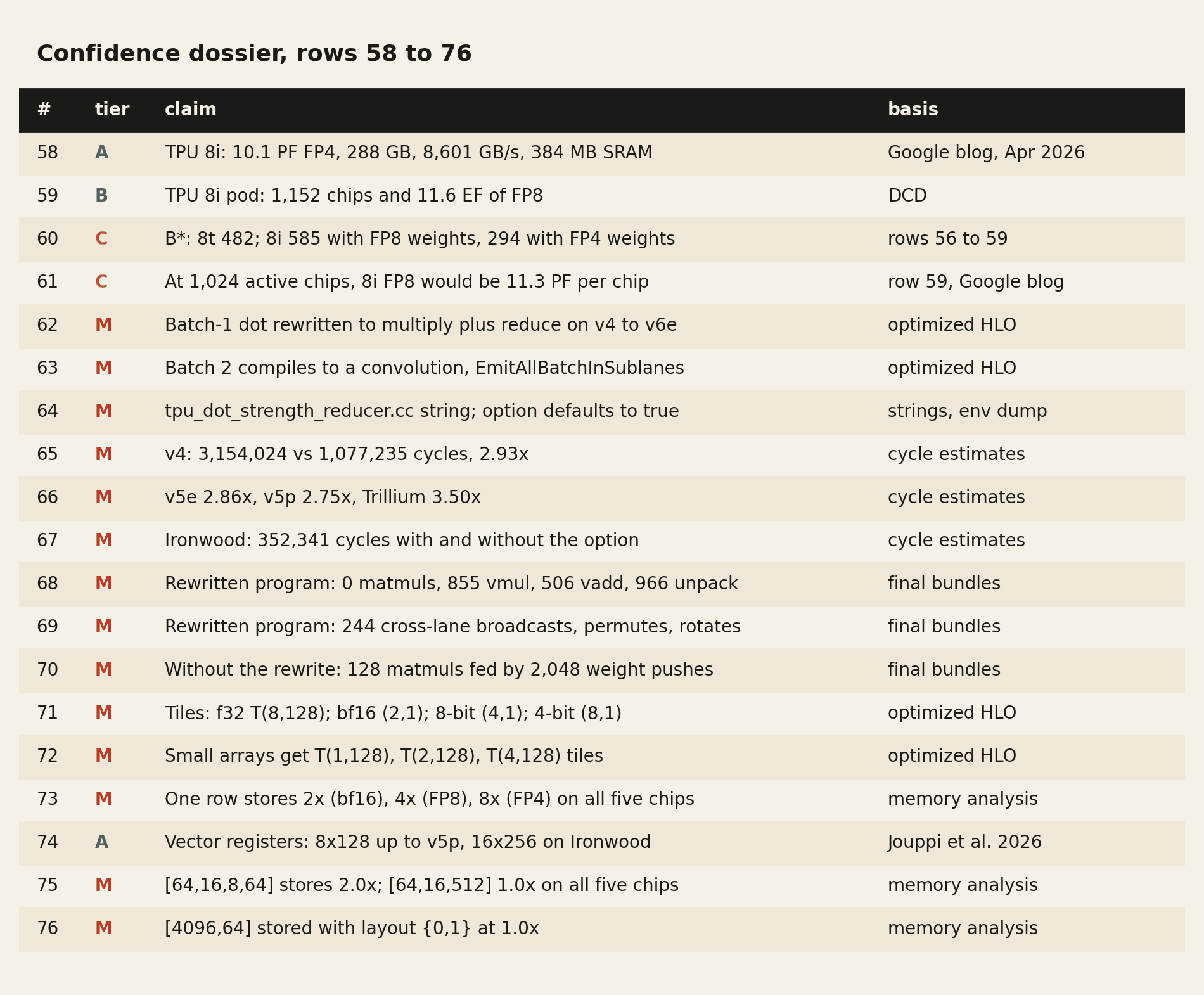
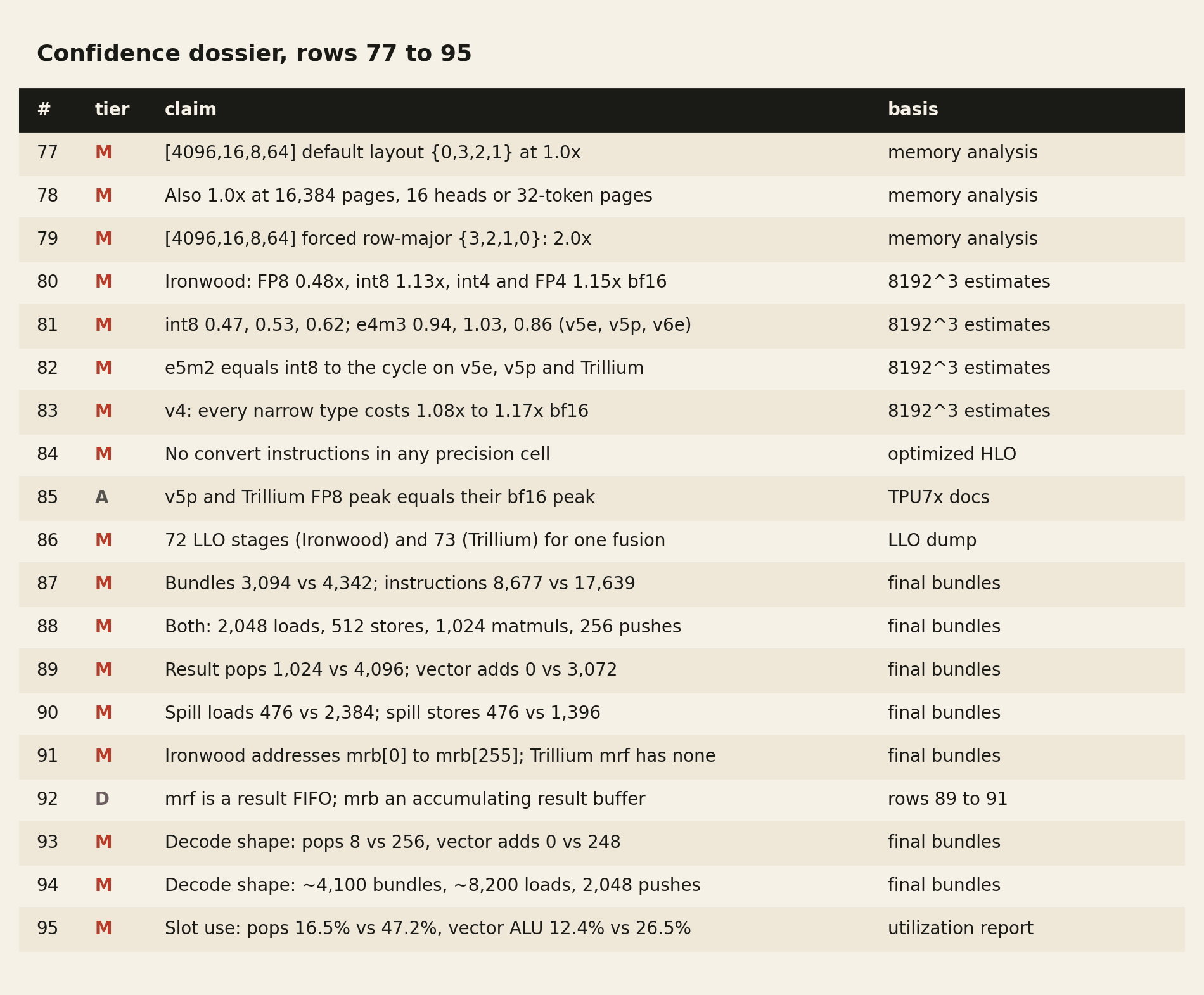
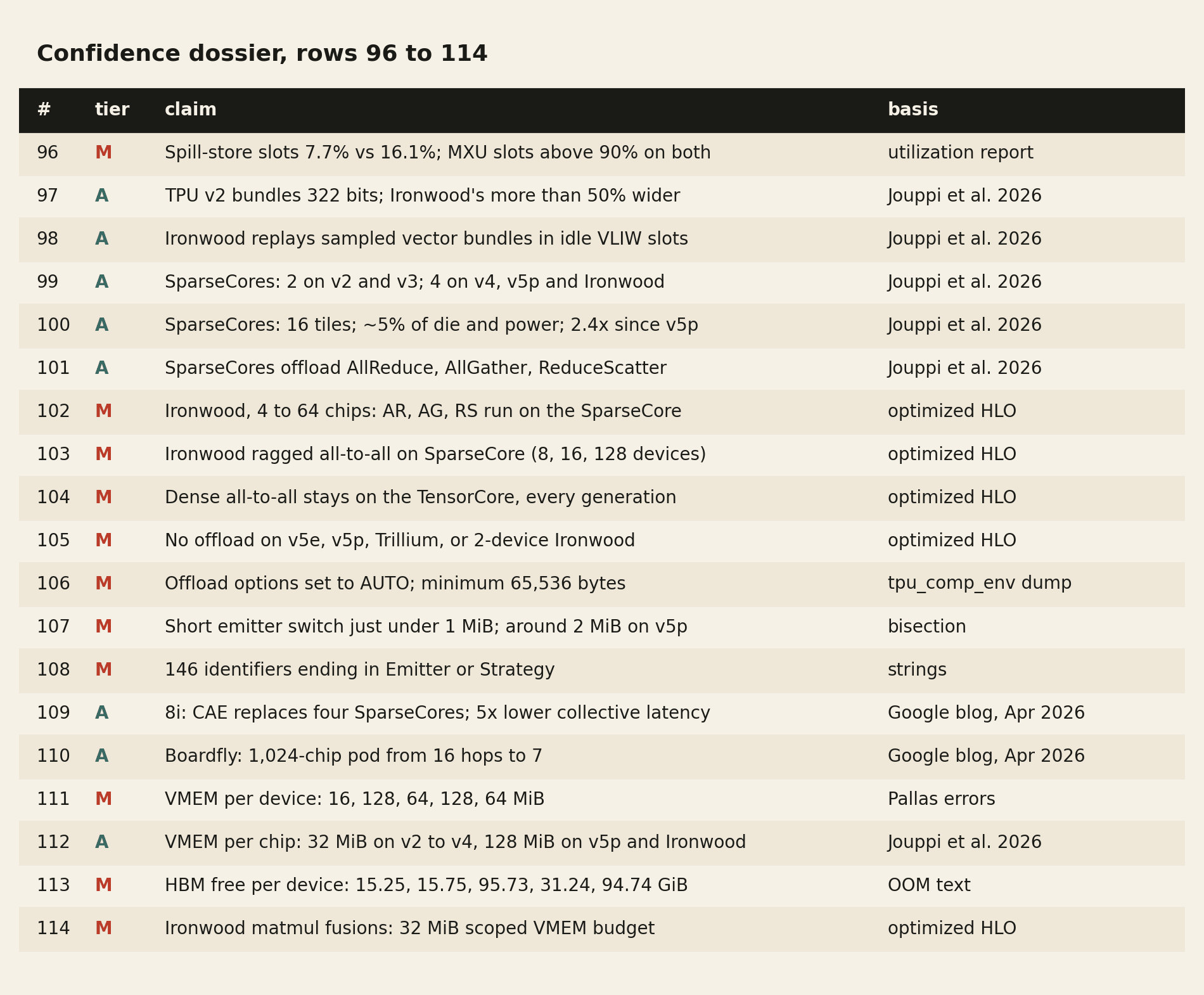
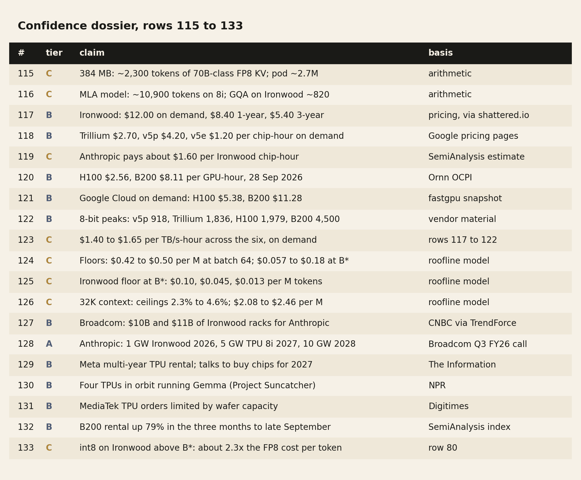
Confidence dossier
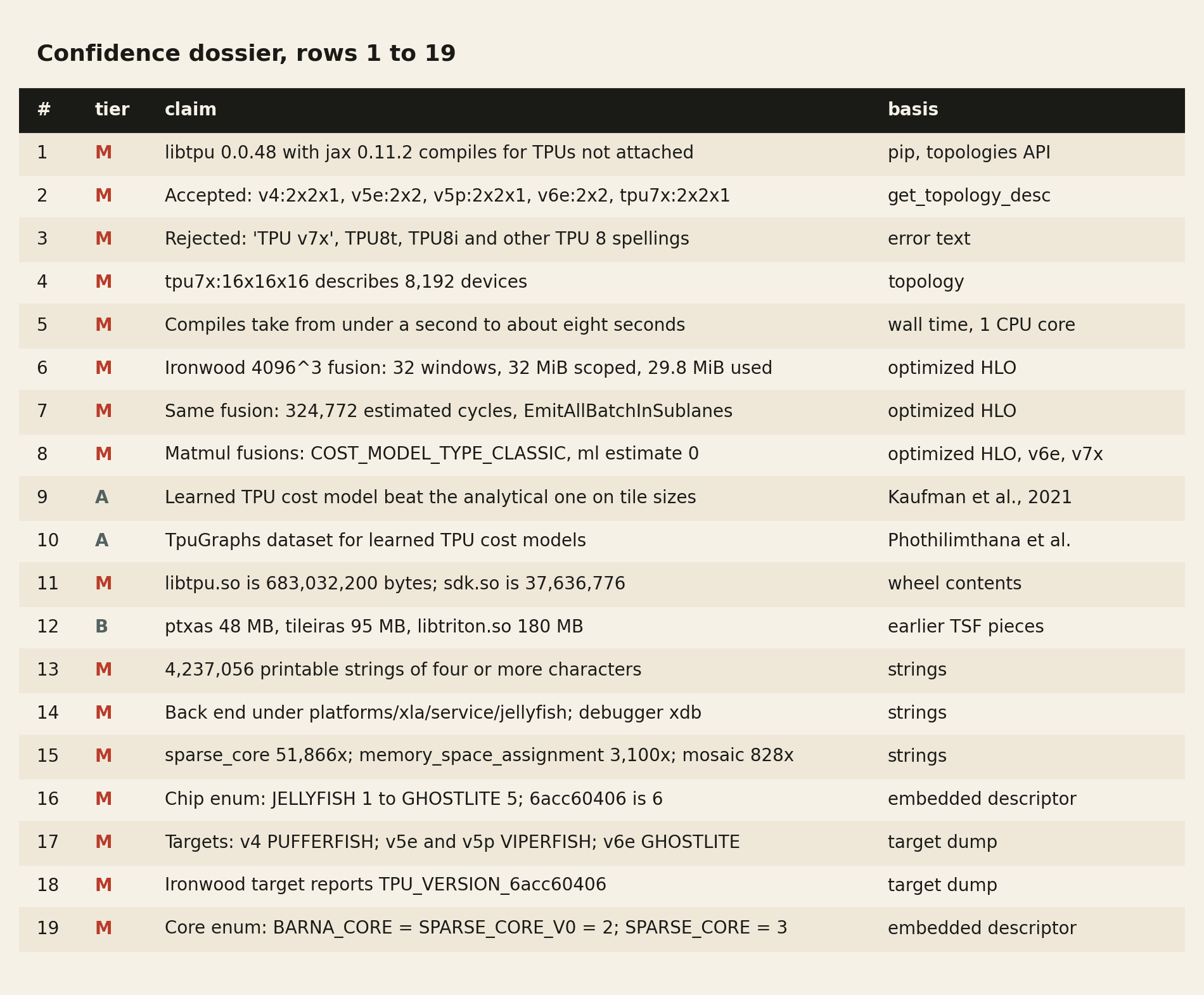
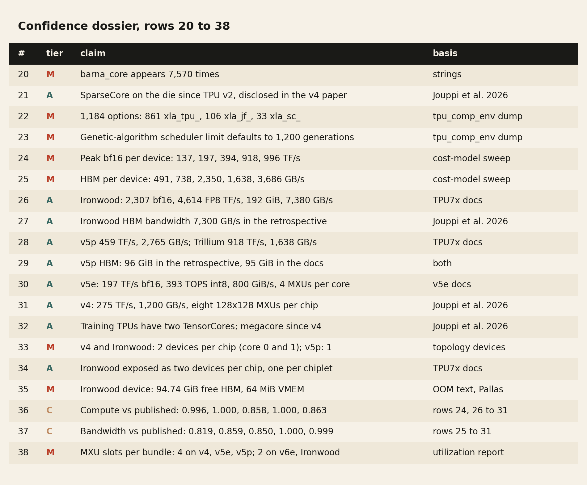
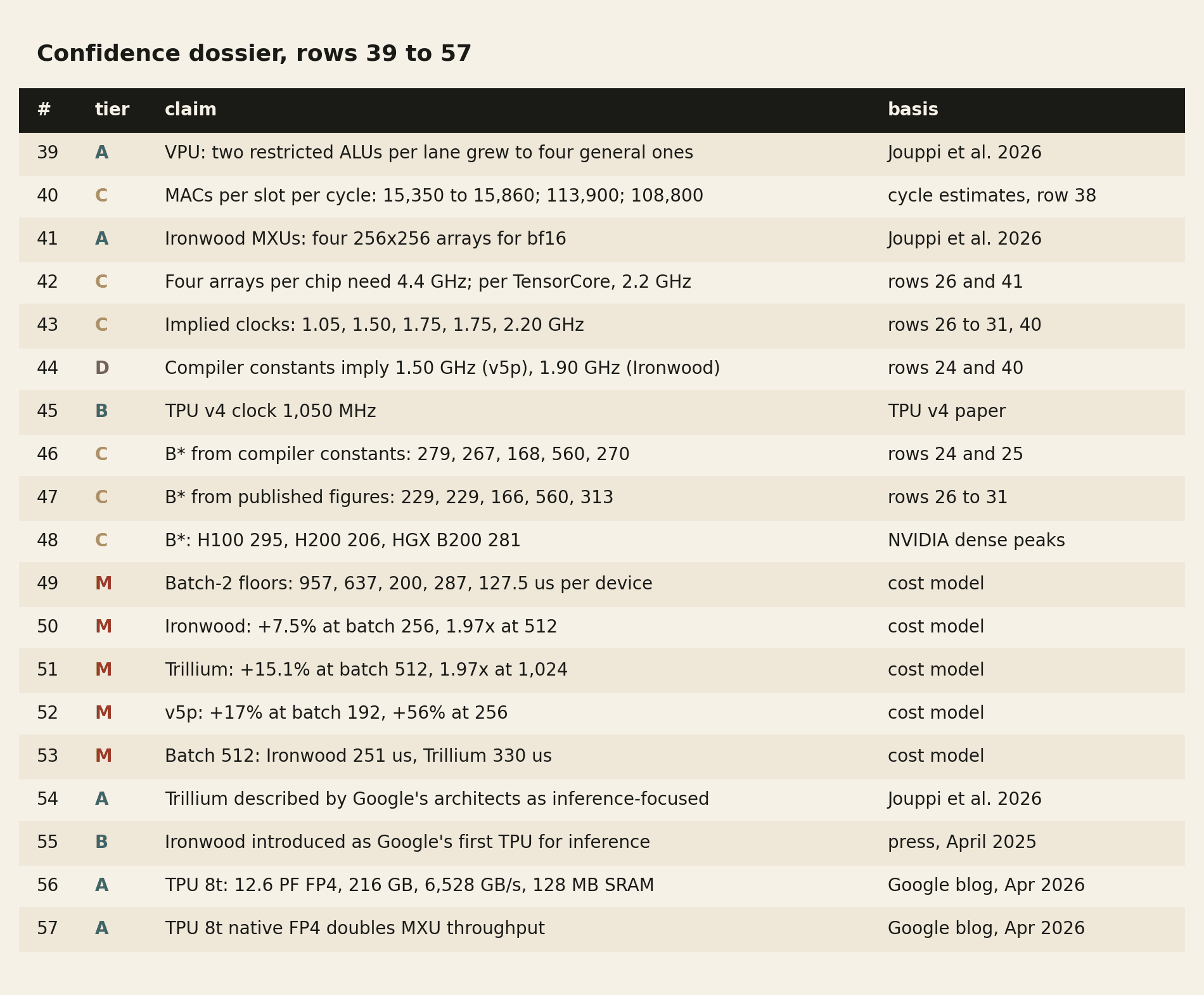
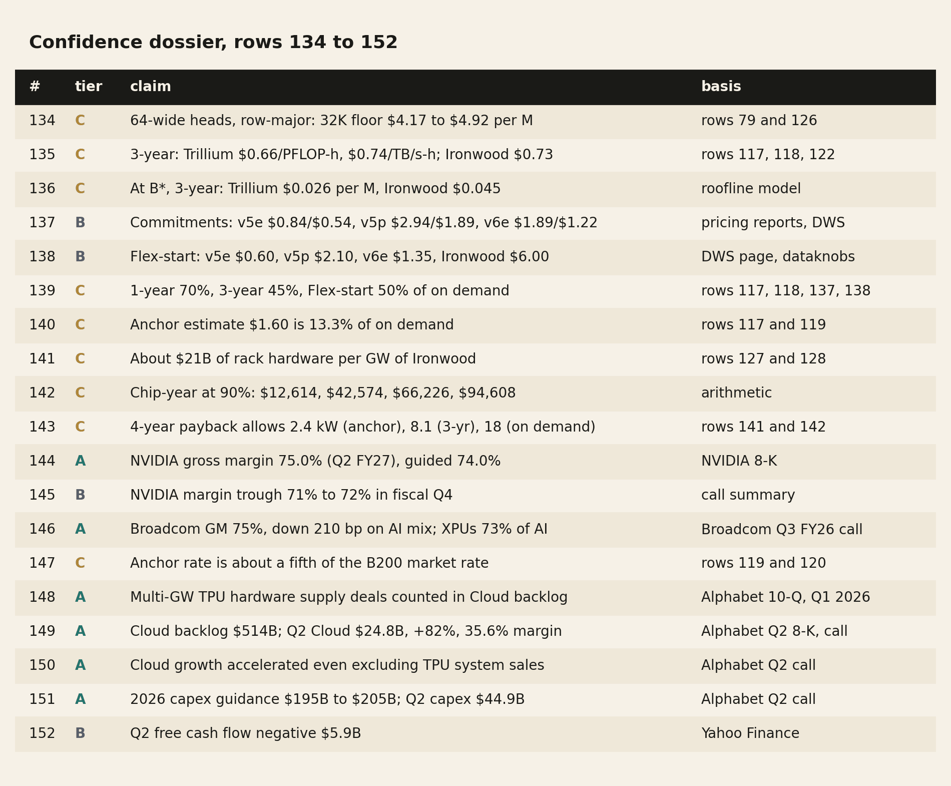
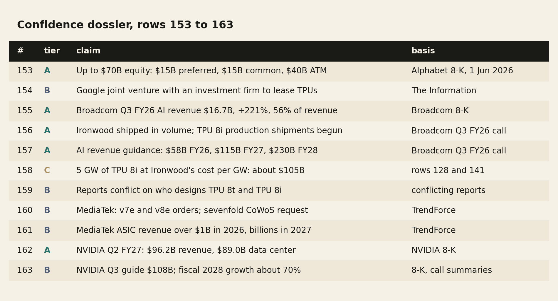
Tier A is a primary document: Google’s documentation, Google’s blog, Google’s architects’ retrospective, a company’s own statement. Tier B is reputable reporting, a published index or a figure from vendor material we did not re-read. Tier C is our arithmetic on A or B.
Tier D is our interpretation. Tier M is our own measurement with libtpu 0.0.48 and JAX 0.11.2 in compile-only mode, with no TPU attached. Every claim in the piece has a row.
Sources
N. P. Jouppi, S. Lakshmanamurthy, C. Young and D. Patterson, “Google’s Training Supercomputers from TPU v2 to Ironwood,” to appear in IEEE Micro, July/August 2026. arxiv.org/abs/2606.15870
Google Cloud, “TPU7x (Ironwood),” Cloud TPU documentation. docs.cloud.google.com/tpu/docs/tpu7x
Google Cloud, “TPU v5e,” Cloud TPU documentation, last updated 11 August 2026. docs.cloud.google.com/tpu/docs/v5e
D. Gupta and S. Mugazambi, “Inside the eighth-generation TPU: An architecture deep dive,” Google Cloud Blog, 22 April 2026. cloud.google.com/blog
HPCwire, “Google Bolsters AI Hypercomputer with New TPU Chips, Virgo Interconnect, Speedier Lustre,” 22 April 2026. hpcwire.com
DatacenterDynamics, “Google unveils eighth-generation TPUs, two dedicated training and inference chips.” datacenterdynamics.com
Moor Insights and Strategy, “Research note: Google TPU 8: Architecture, Context, and Enterprise Relevance.” moorinsightsstrategy.com
N. Jouppi et al., “TPU v4: An Optically Reconfigurable Supercomputer for Machine Learning with Hardware Support for Embeddings,” ISCA 2023. arxiv.org/abs/2304.01433
S. J. Kaufman et al., “A Learned Performance Model for Tensor Processing Units,” MLSys 2021. arxiv.org/abs/2008.01040
P. M. Phothilimthana et al., “TpuGraphs: A Performance Prediction Dataset on Large Tensor Computational Graphs,” 2023. arxiv.org/abs/2308.13490
Google Cloud, “Cloud TPU pricing.” cloud.google.com/tpu/pricing
Google Cloud, “Dynamic Workload Scheduler pricing.” cloud.google.com/products/dws/pricing
shattered.io, “Google Puts $12/Hr Price on Ironwood TPU vs Nvidia,” September 2026. shattered.io
Spheron, “Google TPU v7 Ironwood vs NVIDIA B200: Inference Cost (2026),” citing a SemiAnalysis estimate of Anthropic’s rate. spheron.network
Ornn, Compute Price Index, settlement of 28 September 2026. data.ornn.com/markets
Silicon Data, H100 Rental Price Index (SDH100RT). silicondata.com
fastgpu, “What it costs to rent an H100, B200 or RTX 4090 in September 2026,” DEV Community. dev.to
shattered.io, “Nvidia B200 Cloud Price Hits $8.01/Hr,” on the SemiAnalysis GPU pricing index, September 2026. shattered.io
SemiAnalysis, “TPUv7: Google Takes a Swing at the King.” newsletter.semianalysis.com
TrendForce, “Anthropic Emerges as Broadcom’s Mega-Client; Margin Challenges Ahead,” 12 December 2025. trendforce.com
DatacenterDynamics, “Broadcom bulges with Anthropic AI orders.” datacenterdynamics.com
SDxCentral, coverage of Broadcom’s 2026 earnings call. sdxcentral.com
Dataconomy, “Meta signs multibillion-dollar deal to rent Google TPUs for AI training,” 27 February 2026, reporting The Information. dataconomy.com
Digitimes, “MediaTek TPU orders rise as chip capacity war intensifies,” 1 October 2026. digitimes.com
NPR, “Google launches Project Suncatcher, a step towards AI data centers in space,” 1 October 2026. npr.org
J. Austin et al., “How to Scale Your Model,” Google DeepMind. jax-ml.github.io/scaling-book
JAX documentation, “Ahead-of-time lowering and compilation.” docs.jax.dev
L. Bradanini and L. Tettamanti, “How Blackwell’s Tensor Memory Actually Works,” The Software Frontier, 3 August 2026. thesoftwarefrontier.com
Alphabet, “Alphabet Announces Second Quarter 2026 Results,” Form 8-K exhibit 99.1. sec.gov
Alphabet, Q2 2026 earnings call. abc.xyz
Alphabet, Form 10-Q for the quarter ended 31 March 2026. sec.gov
Alphabet, Form 8-K of 1 June 2026 on equity offerings. sec.gov
Yahoo Finance, “Alphabet Q2 2026 earnings: revenue up 24%, Cloud surges 82%.” finance.yahoo.com
Broadcom, “Broadcom Inc. Announces Third Quarter Fiscal Year 2026 Financial Results,” 2 September 2026. investors.broadcom.com
The Motley Fool, Broadcom Q3 2026 earnings call transcript. fool.com
NVIDIA, “NVIDIA Announces Financial Results for Second Quarter Fiscal 2027,” 26 August 2026. sec.gov
NVIDIA Q2 fiscal 2027 earnings call summary, on margin and fiscal 2028 outlook. transcripts.platformaeronaut.com
TrendForce, “MediaTek Reportedly Secures Google v7e, v8e TPU Orders, Requests 7-Fold CoWoS Increase from TSMC,” 15 December 2025. trendforce.com
TrendForce, “MediaTek Forecasts $1B in ASIC Sales for 2026.” trendforce.com
tech-insider, “Google TPU 8t and 8i: 121 Exaflops, $21B Nvidia Challenge,” with one account of the design-partner split. tech-insider.org
Midas, summary of a Commercial Times report with a conflicting account of the split. getmidas.com
Storyboard18, “Meta signs multi-billion dollar AI chip rental deal with Google,” reporting The Information on a TPU leasing joint venture. storyboard18.com
pump.co, “Google Cloud TPU: Pricing, Performance and Use Cases,” on commitment prices. pump.co
dataknobs, “Google TPU Pricing 2026,” on Ironwood Flex-start and commitment prices. dataknobs.com