
How three companies set the price of intelligence
HBM, the memory wall, and the physics underneath every token. From the capacitor to the income statement.


Author’s note on method. This report was researched in June 2026 against primary sources (JEDEC standards, vendor announcements, supplier earnings releases) and dated trade reporting, with every computed figure derived from first principles and shown inline. The HBM4 ramp, the Rubin and MI450 launches, and the Q1 2026 memory shock are recent events; a verification list of claims worth re-checking sits in Appendix B, with confidence tiers throughout. Two sections present explicit illustrative models (the cost of a stack, the gigawatt chain): their inputs are tagged as sourced or assumed, their arithmetic is exact, and their outputs are ranges, not disclosures. Cross-vendor specifications use published peak figures and are directional where measurement conventions differ. Appendix C specifies the measurement program that would convert several first-principles claims here into original benchmark data. Nothing in this report is investment advice.
The thesis: every token is a memory read
Strip away the software and an output token is a physical event: to produce one token, an accelerator must stream essentially every active parameter of the model from memory through its arithmetic units. A 70 billion parameter model quantized to FP8 is 70 gigabytes of weights.
Generating one token means reading 70 gigabytes. Generating a hundred tokens a second means moving seven terabytes a second, and no amount of arithmetic brilliance changes that requirement, because the arithmetic is not the constraint. During decode, the phase that produces every token anyone has ever read from a model, the limiting resource on every modern accelerator is memory bandwidth.
That bandwidth has exactly one industrial source: High Bandwidth Memory, towers of DRAM dies thinned to thirty micrometers, drilled through with thousands of copper vias, and bonded onto a logic die millimeters from the GPU.
Three companies on earth manufacture it at the frontier: SK hynix in Icheon and Cheongju, Samsung in Pyeongtaek, and Micron in Boise, Hiroshima, and Taichung. Which means the marginal cost of intelligence, the dollars per million tokens that every API price and every AI gross margin ultimately rests on, is set not in Santa Clara but in a three-supplier memory oligopoly, by stacking yields, bonding chemistry, and wafer allocation.
The market has noticed, violently. In the first quarter of 2026, SK hynix posted a 72 percent operating margin, higher than Nvidia’s and TSMC’s most recent reported margins, on revenue that nearly tripled year over year; on the earnings call the company said customer requests for HBM already exceed its planned production capacity for the next three years, per the Q1 release and call coverage.
The supplier of the bottleneck is now more profitable, in percentage terms, than the company whose chips it feeds. That inversion is the subject of this report.
The structure: the device physics that created the wall (II); the wall measured on real silicon, including the operating taxes nobody quotes (III); the anatomy of a stack down to the via, and the yield equation that prices it (IV); the oligopoly’s history and the 2026 supercycle (V); HBM4, the largest architectural break in the technology’s history, now ramping (VI); the machines it feeds and the two opposing design philosophies the new standard revealed (VII); the money, including a transparent cost-per-stack model (VIII); the bridge to the price of a token and the gigawatt-to-wafer chain (IX); the bear case, stated properly (X); the road past HBM4 (XI); and what to watch (XII), with five falsifiable calls.
Two interludes price the KV economy and the power wall along the way. Appendix C specifies the benchmarks that would extend this from synthesis to measurement.
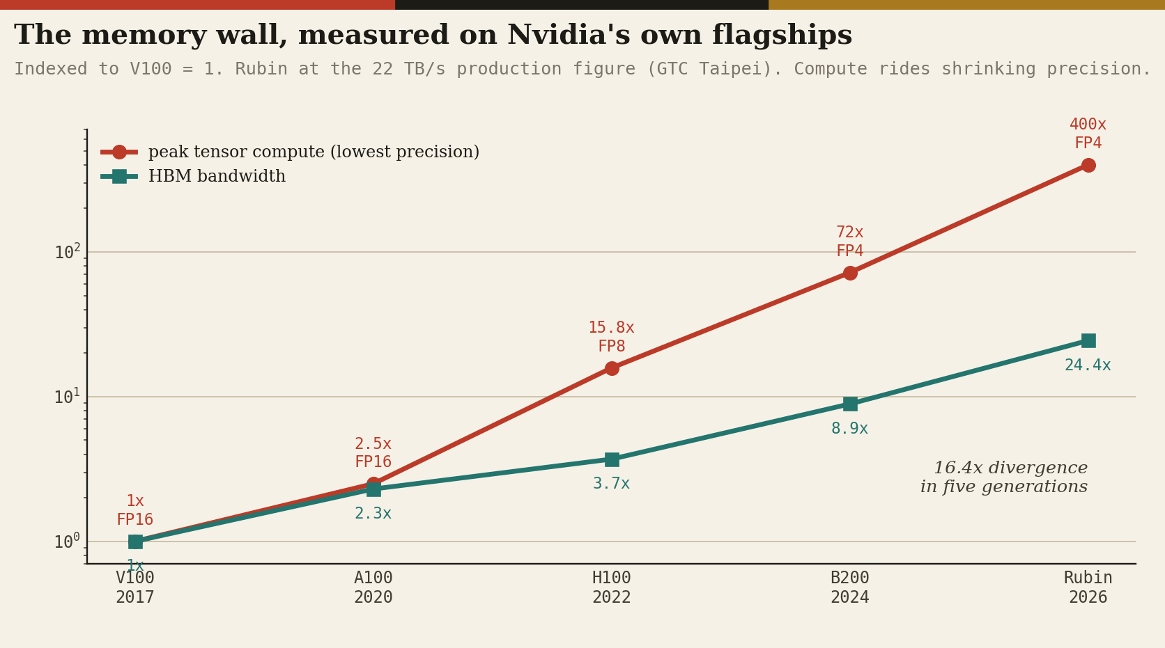
One framing number before the detail. From the V100 in 2017 to the Rubin GPU now entering production, Nvidia’s peak tensor throughput at the lowest supported precision grew roughly 400-fold.
Over the same nine years, the memory bandwidth feeding that compute grew 24.4-fold. The 16.4x divergence between those exponents, computed from the vendors’ own datasheets, is the memory wall. Everything below is downstream of it.
II. The physics: why the wall exists
The wall is not a design oversight. It is the collision of two different scaling regimes, and to price it correctly you have to go down to the cell.
The cell that cannot shrink. A DRAM bit is one transistor and one capacitor, the 1T1C cell, unchanged in concept since 1966. Writing stores charge on the capacitor; reading shares that charge onto a long bitline and asks a sense amplifier to detect the disturbance.
The readable signal is set by charge sharing: the voltage swing the sense amplifier sees is approximately the cell’s stored swing scaled by Cs over (Cs plus Cbl), the cell capacitance against the parasitic bitline capacitance. With modern cell capacitance in the single-digit femtofarads and bitlines loaded by hundreds of neighboring cells, that swing is on the order of tens of millivolts, detected differentially against a reference bitline.
Shrink the capacitor and the signal disappears into noise; the read becomes unreliable; the bit is worthless.
So the capacitor holds a roughly fixed charge requirement regardless of lithography, which is why DRAM capacitors became architecture rather than printing: vertical pillars with aspect ratios beyond 100 to 1, wells drilled a hundred times deeper than they are wide, lined with high-k dielectric laminates (the zirconia-alumina-zirconia family) to wring capacitance from area that no longer exists in plan view.
The consequence is the slowest node cadence in semiconductors. The industry’s DRAM generations crawled from 1x-class around 19 nanometers in the mid-2010s through 1y, 1z, 1a (roughly 14), 1b (roughly 12 to 13) to today’s 1c at roughly 11 to 12 nanometers: a decade to cover what logic crossed in three years.
EUV lithography, which rescued logic, arrived in DRAM late and thinly: SK hynix introduced it at 1a, Samsung uses it on more layers, and Micron famously held out on DUV multi-patterning through 1-beta before adopting EUV at 1-gamma.
Bits per wafer, the quantity that sets the cost of a gigabyte, now improves single-digit percent per year. This is the supply-side bedrock of every price in this report: the raw material of memory has nearly stopped getting cheaper.
The latency that never moved. Hidden under the bandwidth story is a stagnation worse than the capacity one: DRAM row cycle time, tRC, the time to open a row, sense it, restore it, and precharge for the next, has improved by less than 2x in two decades, parked in the mid-40-nanosecond range, because it is governed by the analog physics of sense amplification, not by lithography.
Every bandwidth gain in modern DRAM is therefore parallelism wearing a frequency costume: more banks, more bank groups, deeper prefetch (DDR5 fetches sixteen beats per access), more independent channels, so that thousands of slow rows are in flight at once. HBM is this philosophy at its logical extreme.
The pin that cannot run. The other escape route, faster pins, is capped by signal integrity. A DDR5 pin driving centimeters of motherboard trace through a connector tops out in the high single Gbps; GDDR7 reaches the 30s only over short, exquisitely tuned point-to-point routes at painful energy cost.
And energy is the real currency: moving a bit from a board-level DIMM costs on the order of 10 to 15 picojoules; GDDR-class interfaces sit near 7 to 8; HBM, with its millimeters-long links through a silicon interposer, runs in the 3 to 5 range, and the logic-process base dies of HBM4 push the interface toward 0.75 to 0.8 volts against 1.1 for DRAM-process predecessors, roughly doubling interface efficiency, per TSMC’s published figures (all pJ-per-bit values are approximate vendor-class numbers).
Run the energy arithmetic forward and it bites hard. At 4 picojoules per bit, fully streaming a B200’s 8 TB/s costs about 256 watts; fully streaming Rubin’s 22 TB/s at an improved 3 pJ per bit still costs about 528 watts. Memory traffic alone, at full decode throughput on an HBM4 flagship, plausibly draws two-thirds of what an entire H100 board drew. This is why packages crossed 2,000 watts, why every HBM4 platform is liquid-cooled, and why the JEDEC thermal envelope is now a first-order economic document.
So: a cell that cannot shrink, a row that cannot speed up, a pin that cannot run, and an energy budget that punishes distance. The only move left is the one HBM made: go wide (1,024 wires, now 2,048), go short (millimeters through an interposer), and go up (stack the dies).
Width replaces frequency; proximity replaces drive power; the third dimension replaces the second. The cost of the trick is the subject of section IV: stacking is the most yield-hostile thing the memory industry has ever mass-produced.
III. The wall, quantified, and the taxes nobody quotes
The cleanest way to see the wall is the manufacturers’ own flagship specifications, indexed.
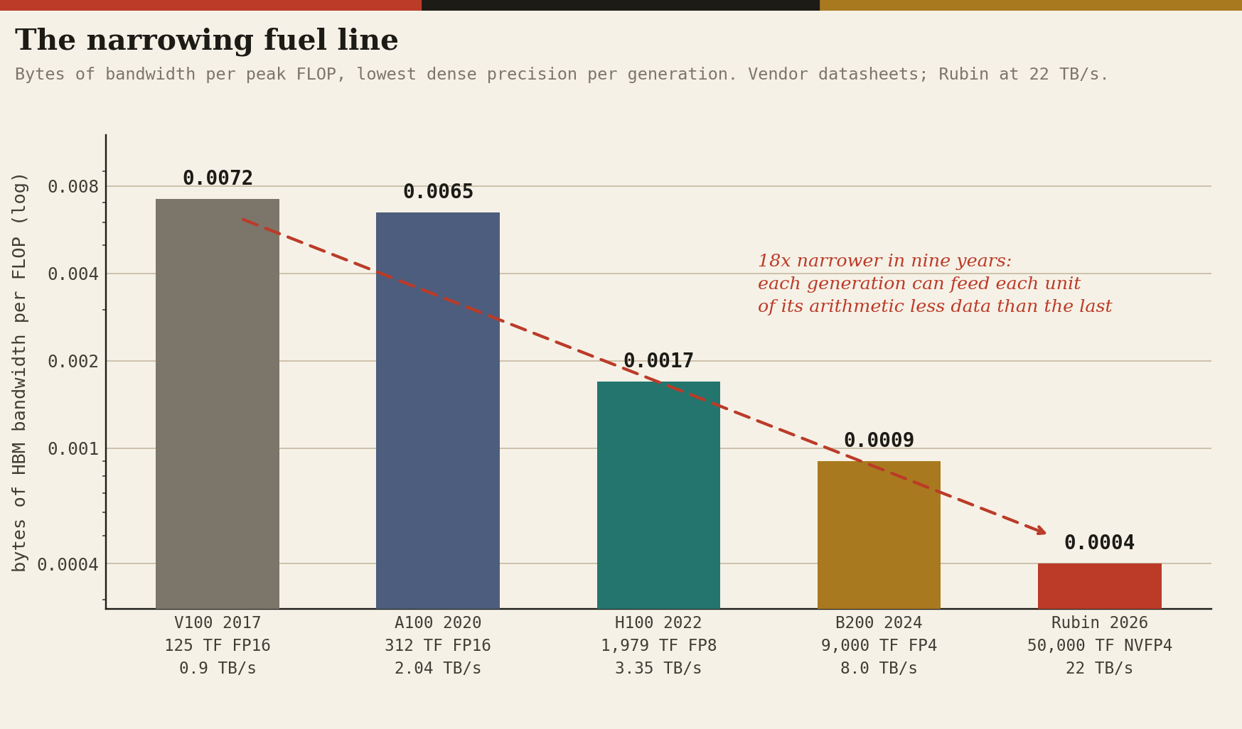
Computed from vendor datasheets and GTC 2026 disclosures. Note that the compute line rides shrinking precision (FP16 to FP8 to FP4), a legitimate but partly definitional gain; the bandwidth line had to be manufactured stack by stack.
The bytes-per-FLOP column is the punchline: each generation can feed each unit of its arithmetic less data than the last. The machine is increasingly a furnace with a narrowing fuel line.
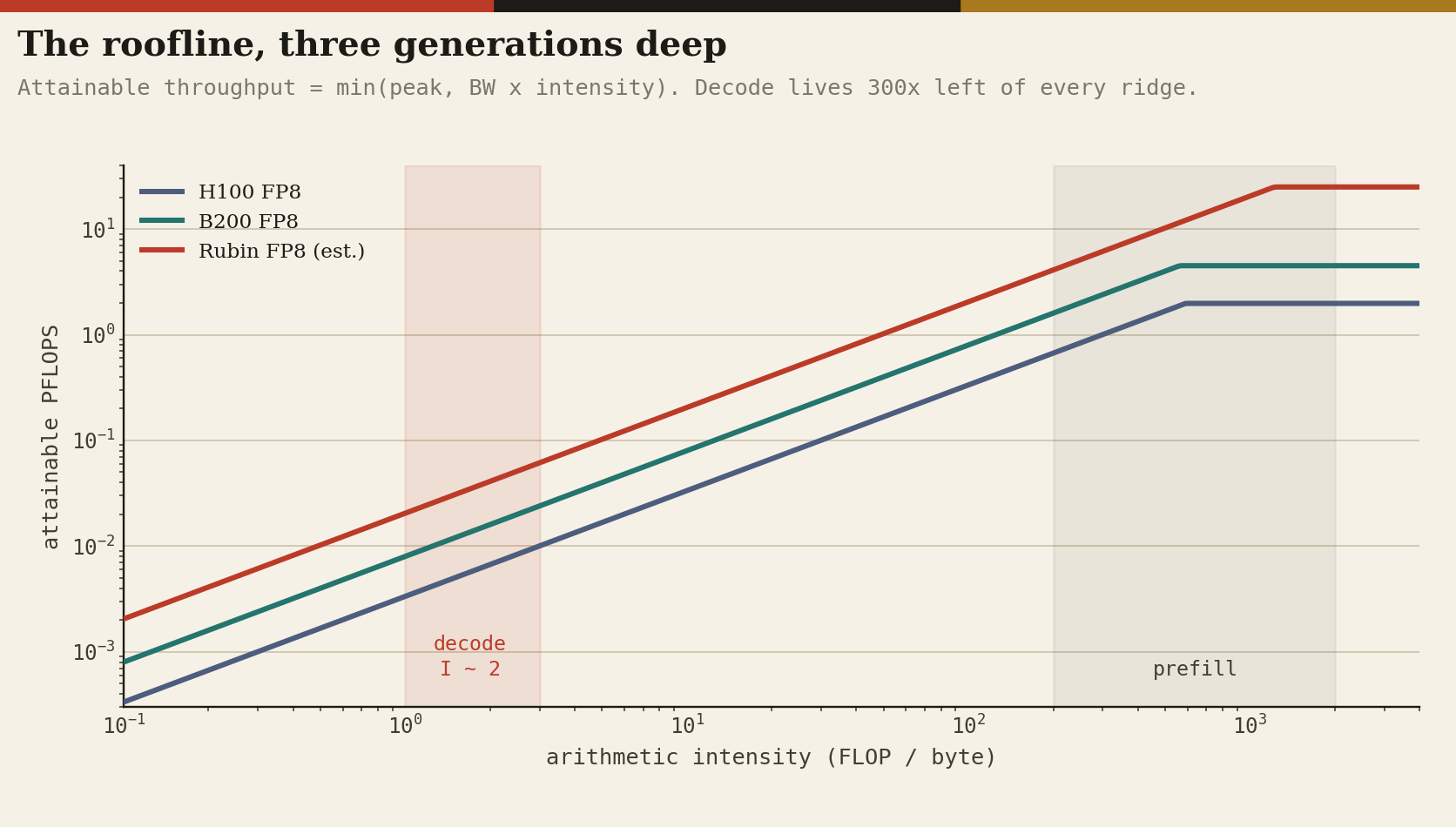
Operationally, the two phases of inference live on opposite sides of the roofline. Prefill is a matrix-matrix multiply with arithmetic intensity in the hundreds of FLOPs per byte: compute-bound. Decode performs roughly two FLOPs per parameter per token while reading every parameter byte: intensity near 2 at FP8, against a ridge point around 560 FLOPs per byte on a B200, so a single conversation idles the arithmetic above 99 percent while it waits on DRAM.
The entire modern serving stack (continuous batching, paged KV caches, speculative decoding, MoE routing) exists to hide that ratio, and every one of those techniques converts the problem into a different demand on the same resource: more concurrent streams need more KV cache, and the KV cache lives in HBM.
Bandwidth sets the speed of a token; capacity sets how many tokens you can be making at once. Both are the stack.
Two operating taxes deserve quantification because they appear in no marketing datasheet.
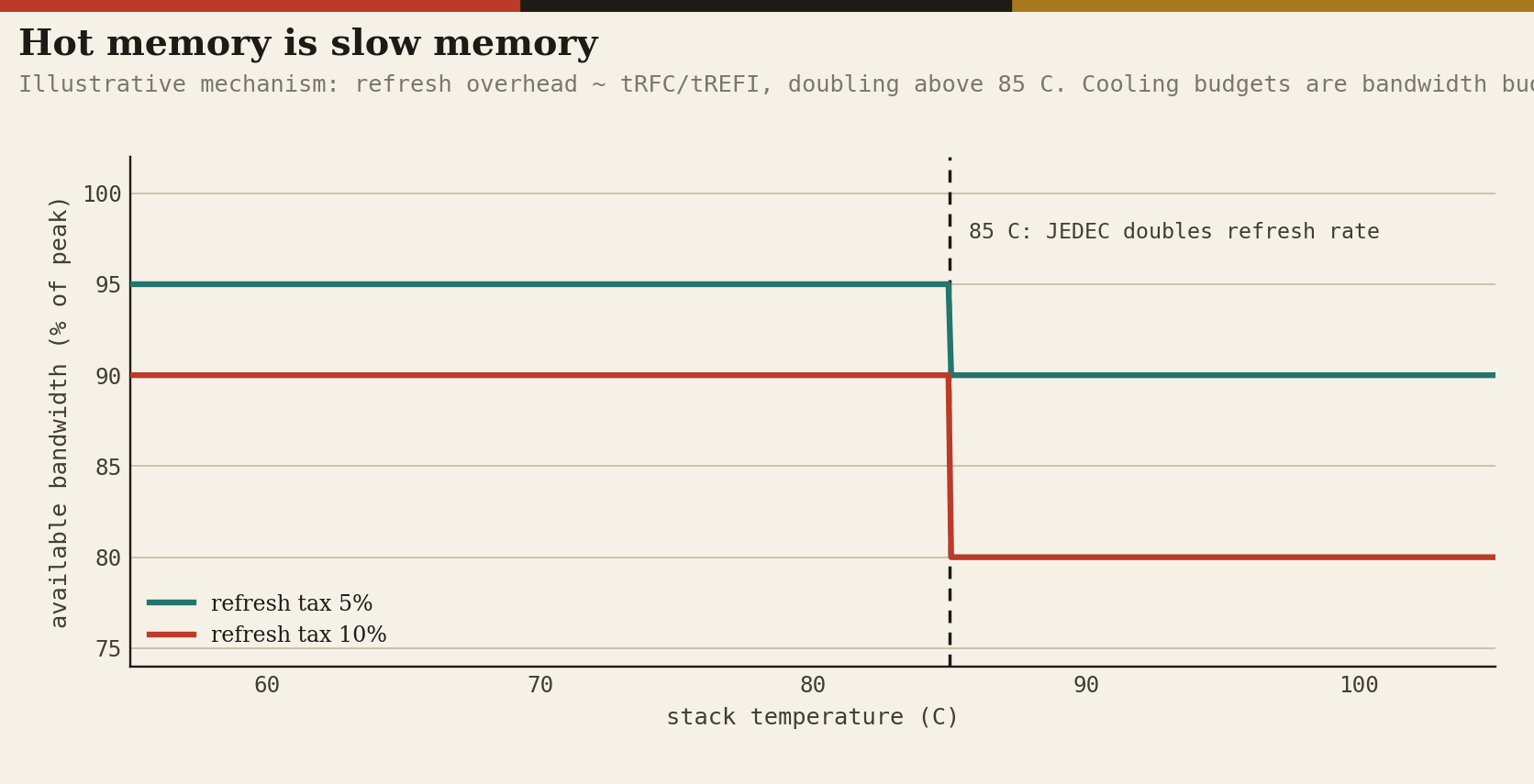
The refresh tax. DRAM forgets; every row must be rewritten on a fixed schedule, and while a bank refreshes it cannot serve traffic. The overhead is roughly tRFC over tREFI, the refresh pulse width over the refresh interval: with multi-hundred-nanosecond tRFC on dense dies against the standard 3.9 microsecond interval, the tax is on the order of 5 to 10 percent of theoretical bandwidth (HBM’s per-bank and managed refresh modes claw some back).
The vicious part is thermal: JEDEC devices double their refresh rate above 85 degrees Celsius, halving tREFI, so the bandwidth tax roughly doubles exactly when the stack is working hardest and hottest. A 16-high tower dissipating tens of watts through molded underfill in a 2,300-watt package is a device engineered to live near that threshold. Hot memory is slow memory, and slow memory is expensive tokens: cooling budgets are bandwidth budgets.
The utilization tax. Achieved bandwidth is not peak. Between refresh, bank conflicts under irregular KV-cache access, read-write turnarounds, and command overheads, well-tuned decode workloads typically realize 60 to 80 percent of datasheet bandwidth (the measurement protocol in Appendix C exists to pin this number per platform).
Every figure in this report that divides by peak bandwidth is therefore optimistic by that factor, uniformly, which preserves comparisons while flattering absolutes.
The wall is also not transient. The longest-baseline study, Gholami and colleagues’ “AI and Memory Wall,” measured twenty years of server hardware: peak compute scaling 3.0x every two years, DRAM bandwidth 1.6x, interconnect 1.4x. Different exponents compound.
The wall is structural, and the industry that gets paid because of it is the next several sections.
IV. Anatomy of a stack, to the via
A current HBM device is a tower: a base die at the bottom and 8, 12, or 16 DRAM core dies above it.
JEDEC’s HBM4 standard, published as JESD270-4 on April 16, 2025, fixes the envelope: a 2,048-bit interface organized as 32 independent channels (each split into two pseudo-channels, 64 concurrent access streams per stack), support for 24Gb and 32Gb core dies in 4-, 8-, 12-, and 16-high stacks, capacities to 64GB per stack, per-pin rates from 8 Gbps in the base spec, and a package height of 775 micrometers for both 12- and 16-high, loosened from HBM3E’s 720 to give 16-high a fighting chance without new bonding physics.
The vertical wiring
Each core die is thinned to 30 to 50 micrometers (SK hynix’s CES 2026 16-high uses 30, about a third of a hair) and pierced by through-silicon vias: copper columns roughly 5 to 6 micrometers in diameter, formed via-middle with deep reactive-ion etch, lined, filled, then revealed by grinding the wafer from the back.
Signal, power, and ground TSVs together number on the order of ten thousand per stack (order-of-magnitude; vendors do not publish counts), with spares woven in: TSV repair logic in the base die can route around dead vias, one of several redundancy layers (alongside row and column fuses) that keep the yield equation below from being even crueler.
Between dies, communication crosses microbump fields at pitches around 25 micrometers, thousands of joints per interface, every one a potential stack-killing defect.
The brain at the bottom
The base die is the stack’s logic: the 2,048-bit PHY facing the host, channel routing, built-in self-test, the IEEE 1500 test wrapper, repair control, and the direct-access port that lets a tester exercise the tower.
Through HBM3E it was built on a DRAM process, because that is what memory firms own, and it shows: DRAM transistors make poor I/O drivers. At HBM4’s 10-plus Gbps per pin across 2,048 lanes, signal integrity demands real logic transistors, real equalization, lower supply rails, which is the engineering reason (beyond the strategic one in section VI) that the base die migrated to foundry logic processes this generation.
How the tower is joined
The bonding step is the deepest process moat in the industry, currently a three-way technology bet.
SK hynix uses MR-MUF, mass reflow with molded underfill: dies are placed and the solder joints formed in a batch reflow, then the whole stack is encapsulated in one molded underfill shot, a flow with better warpage control, a stronger thermal path through the mold compound, and batch throughput, widely credited as the reason it shipped 12-high first and leads yields (the underfill material itself is a quiet chokepoint, long supplied under an exclusive arrangement with Namics, per trade reporting).
Samsung and Micron use TC-NCF, thermo-compression over a pre-laminated non-conductive film: each die is pressed down individually with heat and force, slower and stress-accumulating, but precise at fine pitch.
The bridge step is fluxless TCB, removing flux and its residues by bonding in a reducing atmosphere. The endgame is hybrid bonding: copper pads and dielectric planarized to sub-nanometer roughness, fused face to face with no bumps at all, pitch capability below 10 micrometers, thinner stacks, a direct copper thermal path, and lower parasitics.
It is mandatory somewhere past 16 to 20 layers and brutally hard: Samsung, betting on it most aggressively, was reported in April 2026 to be sampling hybrid-bonded 16-high HBM4 to Nvidia at yields around 10 percent, while SK hynix completed a 12-high hybrid-bonding validation and placed its first inline production order while publicly committing to MR-MUF through HBM4E, per EE Times via TrendForce.
And in April 2026 JEDEC was reported to be weighing a roughly 900-micrometer height for HBM4E, which would let incumbent bonding survive another generation and shift hundreds of millions of dollars of equipment orders with one standards vote.
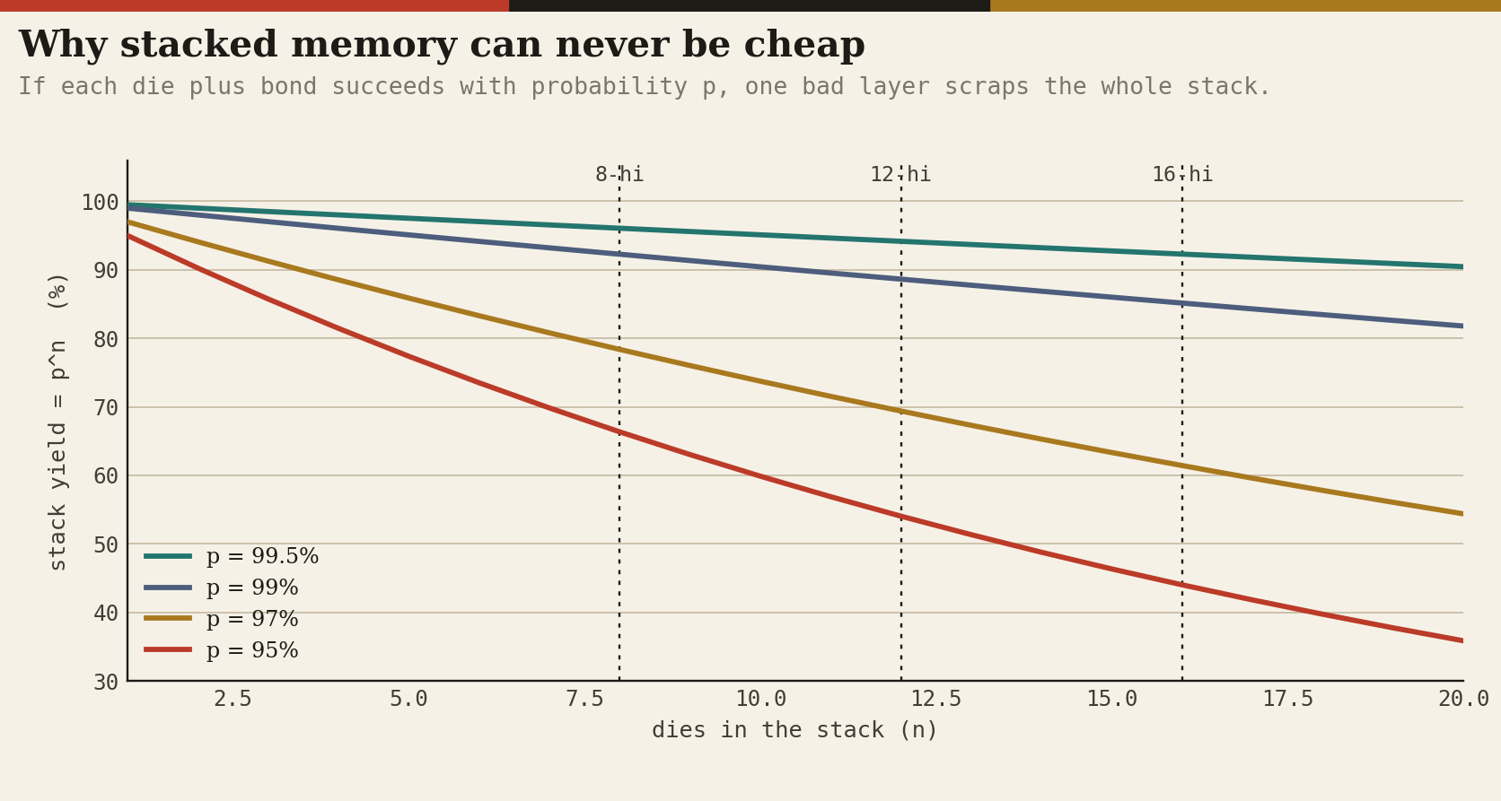
The equation that prices it all
If each die-plus-bond event succeeds with probability p, a stack of n yields p to the power n, and one failure scraps the tower with every good die in it.
At 99 percent per layer, a 12-high yields 89 percent; at 97, 69; at 95, 54. This compounding, mitigated but not repealed by known-good-die testing before stacking, TSV and row repair after, and known-good-stack test at the end (the step driving Advantest’s memory-test boom), is why HBM commands 5 to 6 times the per-bit price of DDR5 (industry trackers put HBM3E near $8 to $10 per GB, roughly $300 per 36GB stack, with early HBM4 stacks around $500, per Silicon Analysts estimates), and why TrendForce calculates HBM consumes roughly three times the wafer area per bit of commodity DRAM once die-size trades and stack losses are counted.
Three suppliers, a decade of bonding chemistry embodied in process recipes, and an exponential that punishes newcomers: that is the moat, stated as math.
V. The oligopoly, and the quarter the memory market broke
HBM was born unwanted. AMD’s packaging architects, led by Bryan Black, spent the early 2010s convincing anyone who would listen that memory belonged on the package; SK hynix co-developed the first standard, and the 2015 Fury X shipped it, 4GB of HBM1 whose capacity ceiling promptly handicapped the card against Nvidia’s cheaper GDDR5 flagship.
The pioneer paid the tuition; the fast follower banked the lesson: Nvidia adopted HBM2 on the P100 in 2016 and never looked back, while for most of a decade the product line survived at SK hynix on conviction more than profit.
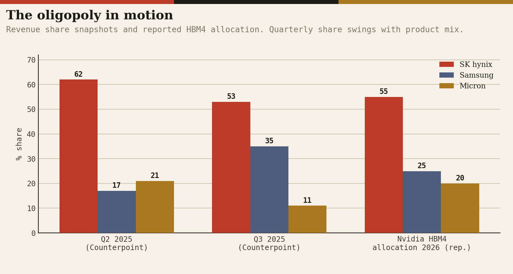
The reward arrived all at once after ChatGPT. SK hynix was first to HBM3 (effectively sole-sourcing the H100), first to 8- and 12-high HBM3E, and converted the lead into a position Counterpoint measured at 62 percent revenue share in Q2 2025, against 21 for Micron, which had skipped HBM3 entirely and leapfrogged to HBM3E, and 17 for Samsung, the incumbent giant caught flat.
We saw repeated Nvidia qualification failures on HBM3E thermals and power through 2024, a leadership change, and a recovery visible by Q3 2025 (Counterpoint: back to 35 percent) that culminated in late January 2026 with Nvidia qualification for HBM4 itself and production from February, per Bloomberg-sourced reporting.
Analyst estimates after Computex put SK hynix at 60 to 70 percent of the HBM4 volume allocated to Vera Rubin, Samsung at 25 to 30, and Micron the remainder, and in early June Nvidia and SK hynix signed a multi-year pact to co-develop AI memory for Rubin and beyond, the first agreement of its kind, which converts the leader’s share into contracted durability, per reporting on the deal; Counterpoint credits SK hynix 61 to 64 percent of the overall HBM market through the period.
Nvidia has also reportedly asked all three for 16-high stacks as early as late 2026.
Then came the quarter that broke the market.
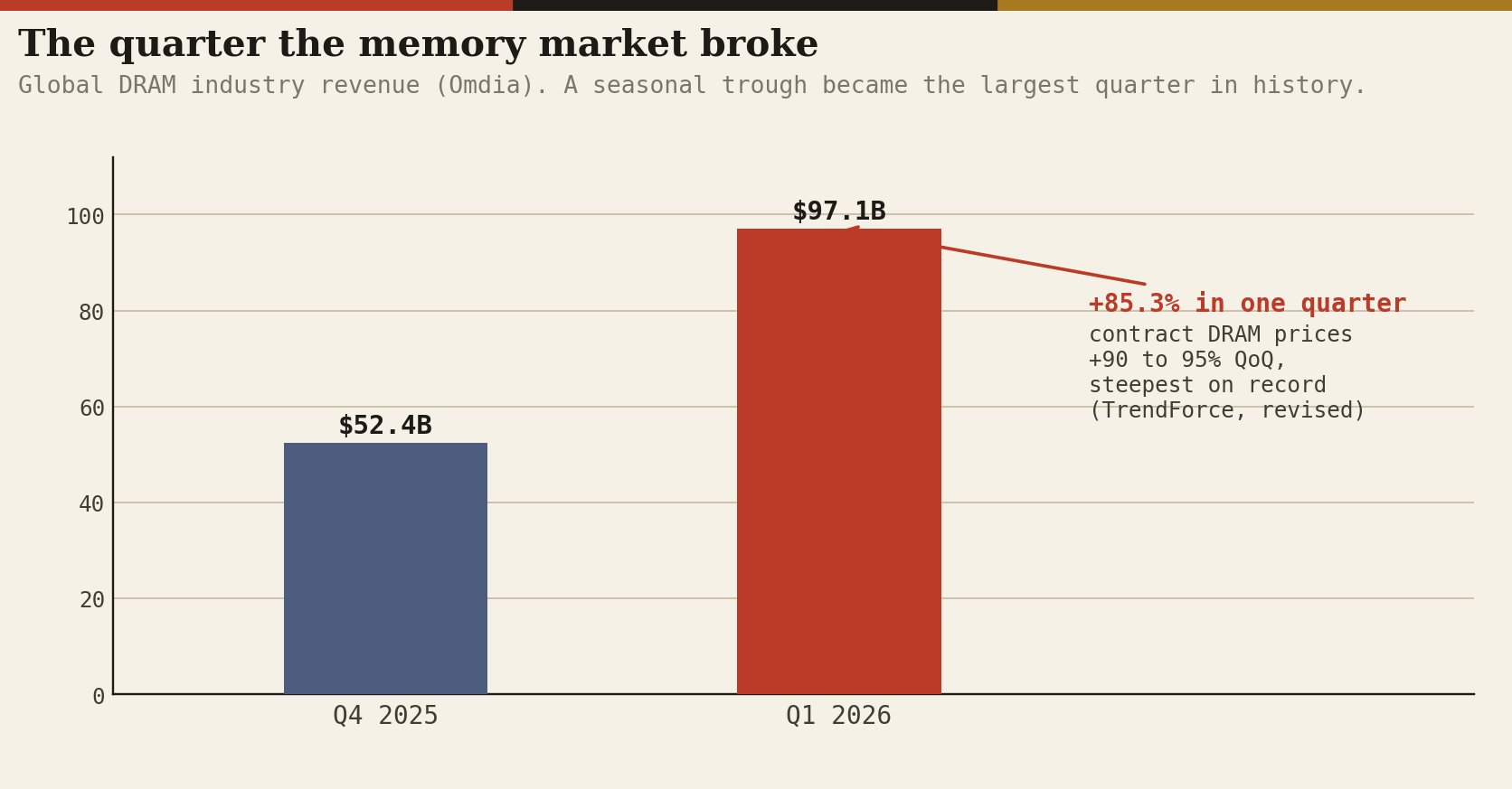
Because an HBM bit consumes about three times the wafer area of a commodity bit and sells for five times the price, every rational fab starved DDR5 to feed it, with DDR4 output collapsing toward 20 percent of 2025 levels; demand met the squeeze, and in Q1 2026, the seasonal trough, global DRAM industry revenue hit $97.1 billion, up 85.3 percent in a single quarter, the largest in history, per Omdia, on contract price increases TrendForce recorded at 90 to 95 percent quarter on quarter, the steepest ever, revised up from an already unprecedented 55 to 60.
The primary-source exhibit is SK hynix’s Q1 2026 report, and it deserves its numbers stated in full because they are the income-statement proof of everything above: revenue of 52.5763 trillion won (about $35.6 billion), the first quarter above 50 trillion in company history, up roughly 60 percent sequentially and 198 percent year over year; operating profit of 37.6103 trillion won (around $25 to 27 billion) at a 72 percent operating margin and a 77 percent net margin, all-time highs on every line, with one quarter’s operating profit nearly matching the whole of record fiscal 2025 (47.2 trillion won) and exceeding all of fiscal 2024, per the company’s release and earnings coverage.
On the call, management said customer HBM requests already exceed planned capacity for the next three years, guided HBM4E samples for the second half of 2026 with 2027 mass production, and announced a 19 trillion won (about $13 billion) advanced-packaging plant, with 2026 capex priorities of the M15X ramp, Yongin site preparation, and EUV tooling.
SK Group’s chairman went further, telling reporters in March that the global wafer shortage will likely persist to 2030 with a shortfall exceeding 20 percent, since capacity takes four to five years to add, per CNBC.
Micron’s fiscal first quarter (the November quarter) had already shown the shape: $13.64 billion of revenue, up 57 percent, 56 percent gross margins, demand “substantially higher” than supply, followed by its December exit from the consumer memory business entirely.
Bank of America frames 2026 as a supercycle on the order of the 1990s boom, with DRAM revenue up 51 percent for the year; the three memory makers added roughly $900 billion of combined market value from September, per market reporting.
Demand now reaches upstream in ways the industry has never seen: in October 2025 OpenAI signed letters of intent with both Samsung and SK hynix under Stargate targeting on the order of 900,000 DRAM wafer starts per month, widely characterized as approaching 40 percent of global output, per Reuters.
Whatever fraction converts, the meaning is the change itself: model companies negotiating two layers down their own supply chain, because they have understood what this report argues. The token supply curve is a wafer allocation.
