



For nine years the register file per SM didn’t grow of a byte, while tensor throughput per clock doubled almost four times. Blackwell’s answer was to take out the accumulator out of the register file, and to put it in an address space with its own allocator, its own barrier, and no coherence with anything. This is what that memory is, what the compiler actually emits for it, and the invariance that explains why it had to exist.
CUDA Mastery 2026
This article is a narrow part of one architecture. The actual guide is the wide one: 34 chapters and thousands words on CUDA 13.x, from memory model up through Hopper and Blackwell tensor cores, written the same way as everything here. Compile it, disassemble it, show the command, then explain what happened.
It also has a corrections page at the end. An early edition listed H100 sparse tensor rates as dense ones, and that single mislabel propagated into three roofline figures before a reader caught it.
That figures are fixed and the mistake is documented rather than quietly removed, which is the standard we would want from anyone selling us a technical book.
Introduction
The very first thing I did with Blackwell was to compile something for it on a machine that has no GPU in it at all. That is not a counter sense.
ptxas, nvdisasm and cuobjdump are ordinary x86 programs, they ship as Python wheels on PyPI, and they will lower PTX for compute capability 10.0 on a laptop with a 40 mb download and no driver. You can’t run the result, but what you can do is to read every instruction, which for my own research, turned out to be the more useful half.
I wanted to know what a tcgen05.alloc costs, first was a small quest, but it got way bigger. It’s important because that’s the instruction that reserves Tensor Memory on Blackwell, it’s in every CUTLASS kernel for the architecture, and every explanation out there said the same three things: it takes a column count, it must be issued by one warp, and the result comes back through shared memory.
Nobody explained in full what the machine does. So, I wrote a small PTX kernel around it, assembled it for sm_100a, and disassembled the result.
What I saw was not an allocation in the sense a systems programmer means: it’s a uniform-datapath atomic against a per-SM pool, wrapped by the compiler in a spin loop with a NANOSLEEP backoff, guarded by three distinct trap handlers that ptxas injects on your behalf, with names like __cuda_sm10x_tcgen05_guardrail_trap_unallocated_columns_being_dealloced.
The tensor cores now have a memory allocator, with contention, with a retry path, and with a compiler-inserted runtime safety checker for use-after-free.
That’s the shape of the thing this article is about. Blackwell added an address space with its own instruction family, not just a cache with its own bus. On top of it we have its own allocator, a barrier, its own access-permission model, and zero coherence with anything else on the chip.
Almost everything written about Blackwell treats Tensor Memory as an implementation detail of the new MMA, but I found out it’s the opposite.
The MMA changed because the memory changed, which consequentially changed due to an arithmetic problem that had been building since 2017, and the consequences run outward through occupancy, epilogue design, quantization format choice, kernel portability, and eventually the cost per million tokens of anything you serve on hardware.
Neither of us owns a B200, unfortunately. Everything here that is measured was measured with a toolchain and a disassembler and is reproducible from the appendix. Derived things are in the open with the arithmetic on the page. All data taken from somebody else’s hardware is attributed and tiered in a dossier at the end.
Where the published literature and our disassembly disagree,(spoiler alert: in two places they do) both are shown.
The number that did not move
We write this very often: every streaming multiprocessor NVIDIA has launched since Volta has exactly 65,536 registers of 32 bits. That is 262,144 bytes of register file per SM, and NVIDIA’s own tuning guides give the same 64 K figure for Ampere and, in the Blackwell tuning guide, for compute capability 10.0.
The same documents states the 255 register per thread ceiling, which we’ll see in use. what we have is: five architectures, three process nodes, four HBM generations, and the largest piece of storage in the SM has not changed capacity by one byte in nine years.
Over the same period tensor throughput per SM per clock went up eight times, and the doubling is exact rather than approximate; NVIDIA’s own numbers make this easily checkable without trusting anybody’s marketing.
A Volta tensor core does 64 fused multiply-adds per clock, eight of them per SM, so 1,024 FP16 FLOPs per clock per SM. Ampere doubled it to 2,048, then Hopper doubled it again to 4,096.
Multiply those out and the datasheets fall out to three digits: 108 A100 SMs times 2,048 times 1.410 GHz is 312 teraflops, which is exactly the published A100 figure. 132 H100 SXM SMs times 4,096 times 1.830 GHz is 989.7 teraflops against a published 989.4.
Run the same identity backwards on Blackwell. The B200 is two dies of 80 SMs with 74 enabled on each, so 148, and 2.25 petaflops dense FP16. That requires 8,192 FLOPs per clock per SM at 1.86 GHz.
Another doubling, and not only ours: the authors of the JAX scaling book run the same division and land on 2,048 FLOPs per tensor core per cycle across four tensor cores per SM, which is the same figure. So the ratio that actually matters, register file bytes per FP16 FLOP per clock, has fallen from 256 on Volta to 32 on Blackwell.
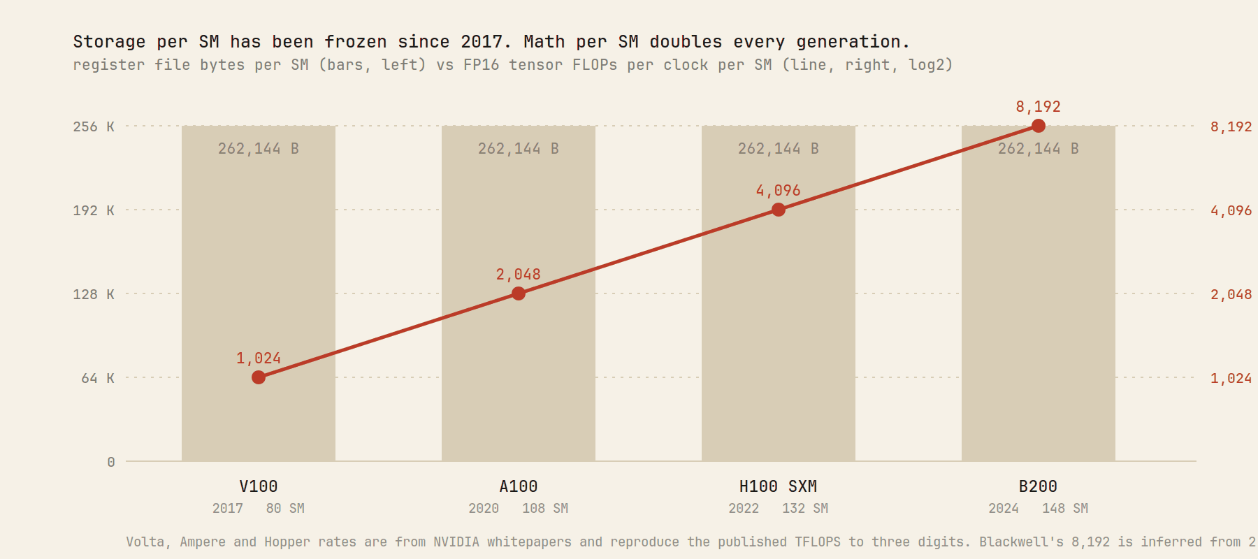
Figure 1. Register file capacity per SM against FP16 tensor throughput per SM per clock. The bars are flat by architectural fact. The line doubles every generation. Register file bytes per FLOP per clock: 256, 128, 64, 32.
You can absorb a gap like that for one generation by being clever, and NVIDIA did, twice. Ampere added asynchronous copy so global to shared traffic stopped passing through registers.
Hopper added the Tensor Memory Accelerator so the address arithmetic for a tiled copy stopped consuming a warp’s registers, and added setmaxnreg so a producer warpgroup could donate its register budget to a consumer at runtime. Both are the same move: find something sitting in registers for no good reason and evict it.
By Hopper the evictable things were gone. What remained was the one thing that genuinely belongs to the math: the accumulator.
The tile that cannot exist
Here is the constraint that decided Blackwell’s design, and it is a single line of arithmetic against a limit you can make the assembler confirm.
On Hopper, wgmma.mma_async accumulates into registers owned by the 128 threads of a warpgroup. The largest shape is m64n256k16. That accumulator is 16,384 FP32 values, which over 128 threads is 128 registers per thread.
As stated in the subtitle, the architectural ceiling is 255, and ptxas will tell you so directly:
$ ptxas -arch=sm_100a -maxrregcount=255 probe.ptx -o /dev/null
$ ptxas -arch=sm_100a -maxrregcount=256 probe.ptx -o /dev/null
ptxas warning : Too big maxrregcount value specified 256, will be ignored
So Hopper’s largest MMA already spends half of every thread’s addressable register space on the output tile, before any addressing, predication, loop state or epilogue arithmetic.
Now… let’s double it, which is what tcgen05.mma does. The largest single-CTA UMMA atom is m128n256k16, twice the area of the largest WGMMA atom. Its accumulator is 32,768 FP32 values. Over a warpgroup that is 256 registers per thread, against a ceiling of 255.
Blackwell’s headline matrix instruction produces a result that is, by one register, unrepresentable in the programming model of every NVIDIA GPU that came before it.
This is a representability problem and not a turning tradeoff. There is no register allocation, no spill policy, no compiler heroics that make a 128 by 256 FP32 tile live in the fragments of a warpgroup, because the fragment model tops out below the tile.
If you want that instruction to exist, its output must go somewhere that is not the register file. Everything else about Tensor Memory follows from that sentence.
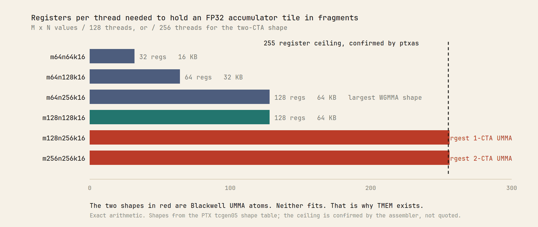
Figure 2. The forcing function. Hopper’s largest MMA already spent half the addressable register space per thread on the output tile. Blackwell’s largest single-CTA MMA needs one register more than the architecture allows.
There is a second argument in the same direction, less absolute but more expensive in practice. A register is thread-private, so an MMA that accumulates into registers is an operation the owning threads must be present for.
On Hopper this is a scheduling tax: a warpgroup issues wgmma, and although the instruction is asynchronous, that warpgroup cannot go and do something else with those registers, because the registers are the accumulator.
Warp specialization on Hopper is largely a set of arrangements to ensure the warps holding accumulators are not the warps doing anything interesting. Move the accumulator out and the whole class of tricks becomes unnecessary.
What Tensor Memory actually is
Tensor Memory is 256 kilobytes per SM, organized as 128 lanes by 512 columns of 32 bit cells. A TMEM address is a 32 bit word whose high 16 bits are the lane index and low 16 bits are the column index. It is not a linear address space with a base and an offset, cause it’s a coordinate.
One consequence worth internalising before reading any CUTLASS TMEM layout: a stride of 65,536 in a TMEM tensor is not a large jump in memory, it is a step of exactly one lane.
Four properties matter more than the capacity, and none are properties of any other memory on the chip.
It is allocated, not addressed. You call
tcgen05.allocwith a column count, which must be a power of two and at least 32, and the hardware returns a base address which it writes into shared memory for you. Allocation is by column, and a column is all 128 lanes: there is no way to reserve part of one. You free it withtcgen05.dealloc, from the same warp that allocated it, or the columns stay claimed.Nothing computes on it. The only instructions that touch TMEM are the
tcgen05family. No ALU op, nold.shared, noldmatrix, nocp.async, no atomic, no texture path. Every pre-processing step happens before data enters and every post-processing step after it leaves. TMEM is the one memory on a Blackwell SM that a general purpose instruction cannot see.Access is partitioned by warp, in hardware. When threads read or write TMEM explicitly, warp 0 of a warpgroup reaches only lanes 0 to 31, warp 1 only lanes 32 to 63, and so on. This is the access model, not a guideline. One warp physically cannot read a full 128 lane accumulator tile, so draining one requires a whole warpgroup by construction, and CUTLASS’s
make_tmem_copyis hardcoded to four warps for exactly that reason.It is a per-SM pool with a hard ceiling. 512 columns, shared by every CTA resident on that SM, and the largest UMMA accumulator occupies exactly 256 of them.
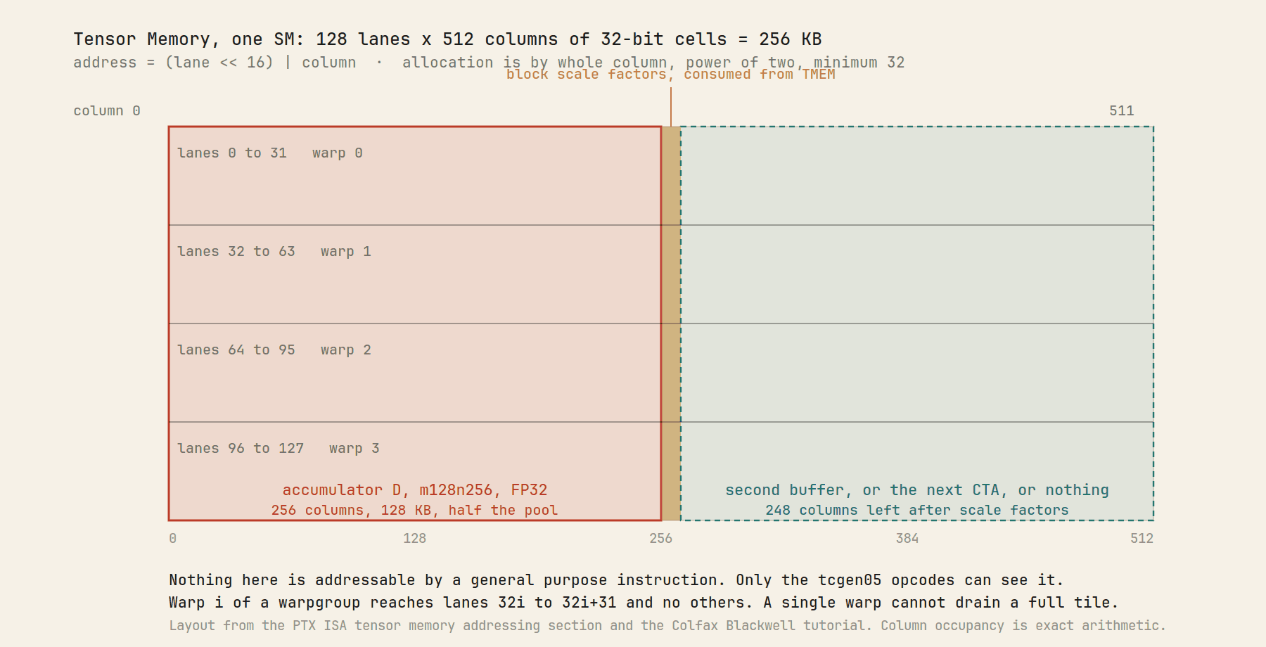
Figure 3. The ledger. Every Blackwell GEMM kernel is, underneath, a plan for carving up 512 columns. The largest accumulator takes half, block scale factors take a few more, and what is left is what you have for pipelining or for a second resident CTA.
The instruction that uses all this is tcgen05.mma, which CUTLASS calls UMMA. Its operand rules invert everything before them. Operand A may be in shared memory or in Tensor Memory. Operand B has to be in shared memory. The accumulator must be in Tensor Memory. Registers appear nowhere in that sentence.
And it is issued by one thread. Not a warp, not a warpgroup: a single elected thread on behalf of the whole CTA, or of a pair of CTAs under cta_group::2, where two SMs sharing a texture processing cluster cooperate on one logical tile.
The consequence is visible in CUTLASS: the CuTe atom’s ThrID, which was Layout<_32> for warp-level MMA and Layout<_128> for Hopper’s warpgroup MMA, is now Layout<_1>, and the thread layouts have been repurposed as layouts of the CTAs collaborating on the instruction.
The abstraction the entire programming model is named after has been vacated at the top of the pipeline. There is still a thread. It does not do the math, does not own the inputs, and does not own the result.
What the compiler actually emits
This is the part we did ourselves, so it is the part we trust most. The toolchain is three PyPI wheels and no GPU: ptxas 12.9.86 from nvidia-cuda-nvcc-cu12, and nvdisasm and cuobjdump 13.3.73 from their standalone packages. The full command sequence is in the appendix.
The probe does the minimum honest thing: reserve 128 columns of Tensor Memory, read back the base address, issue one UMMA into it, commit through an mbarrier, drain one fragment to registers, store it, free the columns.
// probe.ptx, assembled with ptxas 12.9.86 for sm_100a
.version 8.6
.target sm_100a
.address_size 64

.visible .entry umma_probe(.param .u64 p_out, .param .u64 p_adesc, .param .u64 p_bdesc)
{
    .reg .b32  %r<16>;   .reg .b64 %rd<8>;   .reg .pred %p<2>;
    .shared .align 16 .b32 tmem_slot[4];
    .shared .align 8  .b64 mbar[1];

    ld.param.u64 %rd1, [p_out];
    ld.param.u64 %rd2, [p_adesc];
    ld.param.u64 %rd3, [p_bdesc];

    mov.u32 %r1, 128;
    tcgen05.alloc.cta_group::1.sync.aligned.shared::cta.b32 [tmem_slot], %r1;
    tcgen05.relinquish_alloc_permit.cta_group::1.sync.aligned;
    ld.shared.b32 %r2, [tmem_slot];

    mov.u32 %r3, 0;
    setp.eq.u32 %p1, %r3, 0;
    tcgen05.mma.cta_group::1.kind::f16 [%r2], %rd2, %rd3, %r3, %p1;

    mbarrier.init.shared::cta.b64 [mbar], 1;
    tcgen05.commit.cta_group::1.mbarrier::arrive::one.shared::cluster.b64 [mbar];

    tcgen05.ld.sync.aligned.32x32b.x1.b32 {%r10}, [%r2];
    tcgen05.wait::ld.sync.aligned;
    st.global.u32 [%rd1], %r10;

    mov.u32 %r11, 128;
    tcgen05.dealloc.cta_group::1.sync.aligned.b32 %r2, %r11;
    ret;
}
Three facts fall out before the disassembler is even involved.
The minimum PTX ISA version is 8.6, which is CUDA 12.8. Below that the assembler names the requirement precisely:
Feature 'tcgen05.alloc' requires PTX ISA .version 8.6 or later. We mention this because at least one widely linked public write-up puts it at 8.4, and 8.4 does not assemble.tcgen05.commitrequires.shared::cluster, and rejects.shared::ctawithState space incorrect for instruction 'tcgen05.commit', even in a kernel with a trivial cluster andcta_group::1. The tensor core completion path is a cluster level mechanism whether or not you asked for a cluster.ptxasdoes not validate the column count, even when it is a compile time constant. We assembled the probe with 16, 48, 96 and 1,024 columns, all of which violate the documented power-of-two and minimum-32 rules, and all of which assembled without a warning. The rule is enforced by hardware at runtime, not by the compiler. Given that the failure mode is a trap handler, this is a class of bug that only exists on a machine you may not own.
The allocator
Here is what tcgen05.alloc becomes. Address arithmetic trimmed, control flow still intact.
// nvdisasm -c probe_sm100a.cubin, excerpt
        ELECT P0, URZ, PT ;
   @!P0 BRA `(.L_x_2) ;
        DEPBAR.LE SB0, 0x36 ;
        UTCATOMSWS.FIND_AND_SET.ALIGN UP0, UR4, UR4 ;      // claim an aligned run of columns
        PLOP3.LUT P0, PT, PT, PT, UP0, 0x80, 0x8 ;
        SEL R0, RZ, 0xffffffff, !P0 ;
        ISETP.NE.AND P0, PT, R0, RZ, PT ;
    @P0 BRA `(.L_x_3) ;                                    // claimed, continue
.L_x_4:
        NANOSLEEP 0x64 ;                                    // back off, then retry
        UTCATOMSWS.FIND_AND_SET.ALIGN UP0, UR4, UR4 ;
        ...
   @!P0 BRA `(.L_x_4) ;                                    // spin
.L_x_3:
        ATOMS.OR RZ, [UR4], R2 ;                           // record the claimed mask in SMEM
        STS [UR6], R0 ;                                    // publish the base address
        ...
        UVIRTCOUNT.DEALLOC.SMPOOL 0x80 ;                   // SM pool virtual counter
The claim is a UTCATOMSWS.FIND_AND_SET.ALIGN, a uniform-datapath atomic that searches a per-SM pool for a free, aligned run of columns and sets them.
On failure the compiler emits a NANOSLEEP of 0x64 units and retries indefinitely. So a Blackwell kernel that allocates Tensor Memory has a spin loop on its critical path that no source line asked for, and the pool is genuinely contended, otherwise the retry path would not be there.
Then there are the guardrails. ptxas injects three named trap handlers and fifteen references to them, and it does so identically at every optimisation level from -O0 to -O3:
$__internal_0_$__cuda_sm10x_tcgen05_guardrail_trap_col_being_dealloced_not_returned_by_alloc
$__internal_1_$__cuda_sm10x_tcgen05_guardrail_trap_phase_invalid_during_alloc
$__internal_2_$__cuda_sm10x_tcgen05_guardrail_trap_unallocated_columns_being_dealloced
Read those names as a bug taxonomy. Freeing columns you did not allocate. Freeing a column that came from a different allocation. Allocating from an invalid phase.
That is a use-after-free checker, a double-free checker and a state machine assertion, compiled into every kernel, unconditionally. NVIDIA does not do this casually, and the fact that they did it tells you what the failure modes look like in practice.
Why this matters beyond trivia
Every mental model of a GPU kernel assumes resources are assigned at launch. Registers and shared memory are fixed by the compiler and the launch configuration, and occupancy is computed from them before a single instruction runs. Tensor Memory is the first first-class SM resource that is acquired at runtime, can block, can fail, and is arbitrated by an atomic. It moves part of the occupancy calculation out of the launch and into the kernel body, where no static tool can see it.
One number for scale. The probe above, whose actual work is one matrix multiply and one 32 bit drain, compiles to 152 SASS instructions at -O3 and 400 at -O0, using 14 registers and 24 bytes of shared memory.
Two of those 152 are the tensor core; the rest is allocation, election, barrier phase tracking, address reconstruction and guardrails.
The instruction
// dense f16
UTCHMMA      gdesc[UR14], gdesc[UR16], tmem[UR9], tmem[URZ], idesc[URZ], UPT ;
// same source with .sp: the sparsity metadata takes the fourth tmem slot
UTCHMMA      gdesc[UR14], gdesc[UR16], tmem[UR7], tmem[UR4], idesc[UR5], UPT ;
// same source with .cta_group::2
UTCHMMA.2CTA gdesc[UR12], gdesc[UR14], tmem[UR8], tmem[URZ], idesc[URZ], UPT ;
// NVFP4, block16 scaling: scale factors are a fifth tmem operand
UTCOMMA.4X   gdesc[UR14], gdesc[UR16], tmem[UR8], tmem[URZ], idesc[URZ], tmem[UR8], UPT ;
Every operand is a descriptor or a Tensor Memory coordinate, and every one lives in a uniform register, the UR file, not the per-thread register file. The U prefix is the same U as in UMOV, ULEA and UIADD3: the scalar, warp-uniform datapath NVIDIA added in Turing for address arithmetic. Blackwell’s matrix multiply runs entirely on it. There is no vector register in the instruction at all.
That is the cleanest evidence we have found that the CTA, not the thread, is now the unit of tensor computation. It is not an abstraction in CUTLASS or a convenience in PTX. It is visible in which register file the opcode reads.
One clarification the SASS supports and the secondary literature often gets wrong: under cta_group::2 the instruction is not issued by both CTAs in lock step. CUTLASS’s own two-SM tutorial states that only one of the two peer CTAs executes it, and names that one the leader. A single thread, in a single CTA, drives a matrix multiply spanning two SMs.
The dense form passes tmem[URZ], the zero register, in the fourth slot; the sparse form fills it with a real address.
So structured sparsity metadata also lives in Tensor Memory, alongside the accumulator and, for block scaled kinds, alongside the scale factors. Three different kinds of state, one pool of 512 columns.
The opcode family
We compiled the probe once per qualifier and disassembled each result. This mapping is measured.
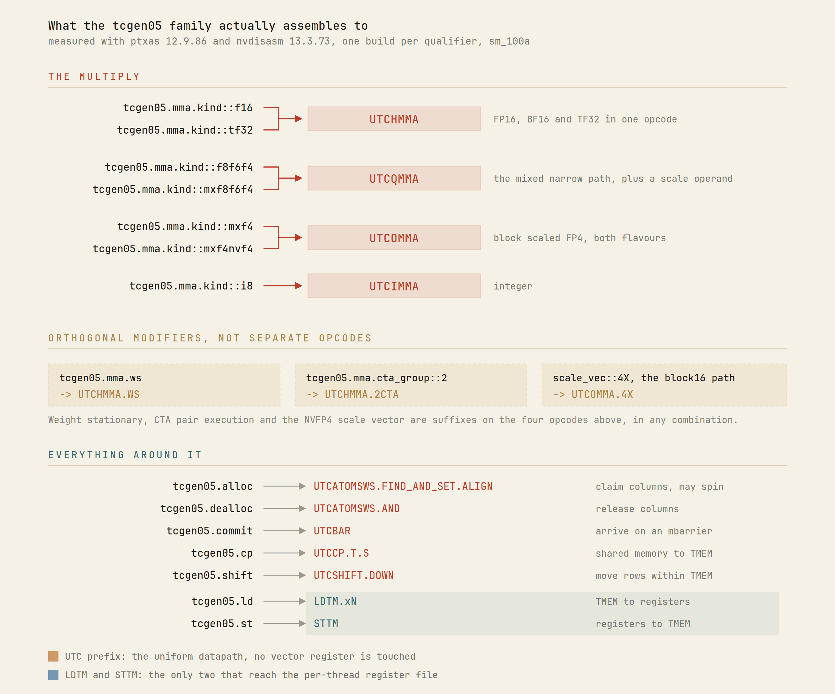
This disagrees with the published literature in one place. The Delaware microbenchmarking paper, which is otherwise the most useful public measurement of this hardware and which we lean on later, reports in its Table IV that tcgen05.mma lowers to HMMA, QMMA, OMMA and IMMA, the same opcode names Volta through Hopper used.
On our disassembly it does not. The distinction is not cosmetic: HMMA reads and writes vector registers, UTCHMMA touches none. The most likely explanation is that the table was written from the family names rather than from a fresh disassembly.
Which chips can run any of this
Compiling against every target the assembler accepts produces a matrix sharper than the marketing, and the sharpest row is the one nobody mentions.
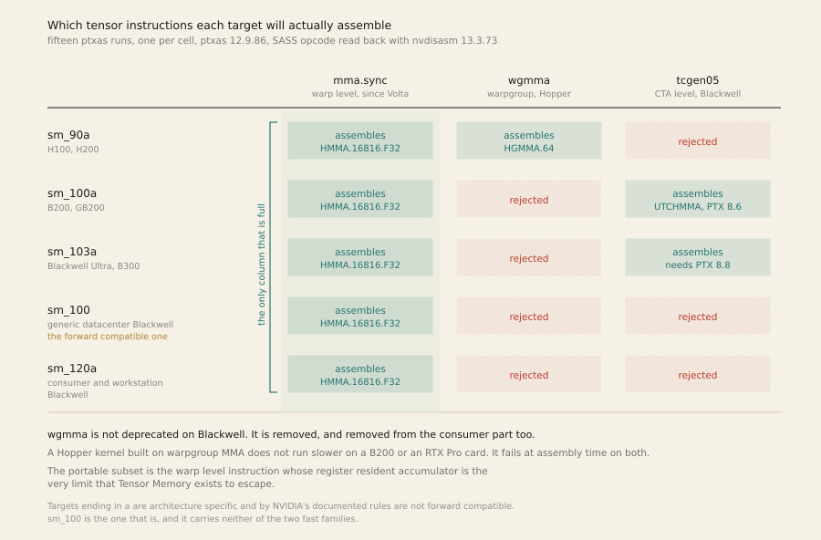
$ ptxas -arch=sm_100  probe.ptx  -o /dev/null
ptxas error : Instruction 'tcgen05.alloc' not supported on .target 'sm_100'

$ ptxas -arch=sm_100a legacy.ptx -o /dev/null
ptxas error : Instruction 'wgmma.fence' not supported on .target 'sm_100a'

$ ptxas -arch=sm_120a legacy.ptx -o /dev/null
ptxas error : Instruction 'wgmma.fence' not supported on .target 'sm_120a'
Three things to take from that table.
First, wgmma is not deprecated on Blackwell. It is removed, and it is removed from every Blackwell target including the consumer one. A Hopper kernel built on warpgroup MMA does not run slower on Blackwell, it fails at assembly time on all of sm_100a, sm_103a and sm_120a.
This is a harder break than any NVIDIA has shipped in the tensor core era, and it is worth stating precisely because the commonly repeated version of this claim, that consumer Blackwell falls back to mma.sync and wgmma, is wrong on the second half. There is no wgmma to fall back to.
Second, sm_100 without the trailing a, the forward compatible target whose PTX a future driver may recompile for a future chip, has neither tcgen05 nor wgmma.
The entire tensor path that defines Blackwell is available only on architecture specific targets, which by NVIDIA’s documented rules are not forward compatible with anything.
Third, the only instruction family that spans Hopper, datacenter Blackwell and consumer Blackwell is mma.sync, the warp-level, register-resident, m16n8k16 class of instruction that predates all of this. That is the portable subset now. It is also the one whose accumulator lives in the register file, which is the constraint we said the architecture outgrew.
The portable path and the fast path have fully separated. What runs everywhere is the instruction whose limits forced Tensor Memory into existence.
The practical consequence is a development loop, not a benchmark. You cannot write, debug or profile a tcgen05 kernel on a workstation. Not slowly, not at reduced fidelity, not at all. The instructions do not exist on hardware you can buy without a data center behind it.
In our compiler moat piece we argued the durable advantage sits at the ptxas and SASS layer and that the counter-technology is research rather than a new language. This adds a cruder second mechanism that has nothing to do with compilers: iteration on the instructions that matter now requires an allocation of scarce hardware.
We should immediately weaken that. The barrier is money and patience rather than access. B200 time is rentable by the hour, and the author of the best tcgen05 tutorial we have read, writing as gau-nernst, reports reaching 98 percent of cuBLAS on a 4096 cubed problem using rented capacity.
A single motivated person got there in a blog series. That is way a much weaker moat than a first reading suggests.
The cost of getting the answer back
tcgen05.ld takes a shape and a repetition count, and the count determines how many 32 bit values land in each thread’s registers.
We swept the count from 1 to 128, forced every loaded value to stay live by storing all of them, and read the allocation from ptxas -v.
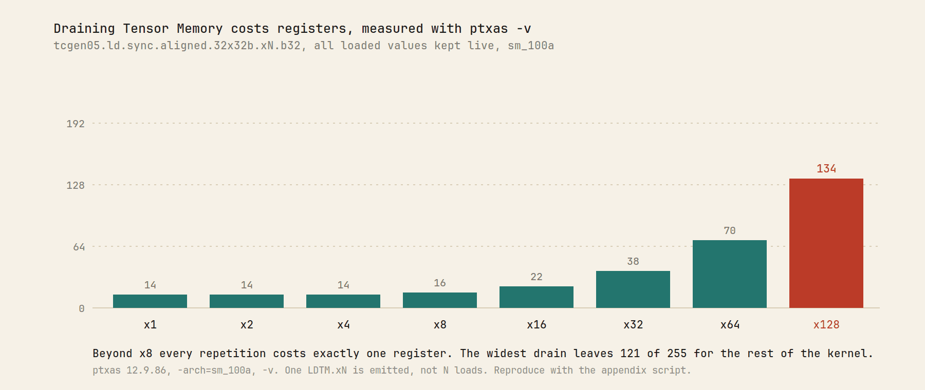
Figure 4 The epilogue tax, measured. A single ldtm.x128 costs 134 registers per thread. Across a warpgroup that is 67 KiB of the 256 KiB register file, just over a quarter of it, checked out purely to hold data on its way from one on-chip memory to another.
The curve is N plus six, and ptxas emits one LDTM.xN rather than N loads. So the register file did not stop being the bottleneck. It stopped being the bottleneck for the multiply and became the bottleneck for the epilogue.
On a Hopper kernel the accumulator is already in registers when you want to scale it, add a bias, apply an activation and cast down. On Blackwell you must first pay to bring it back, and the wider you pay the less room remains to do anything with the result.
Every fused epilogue on this architecture is a negotiation between drain width and register headroom, and no source-level construct expresses it.
Why it had to be a separate memory
previous sections explained why the accumulator left the register file. It does not explain why the destination is a new addressable memory rather than a hidden internal buffer.
For that you need the traffic number, and the traffic number turns out to be more interesting than we expected when we first ran it.
Start with the shape rule, which is the load bearing fact. In CUTLASS’s Blackwell MMA traits the K extent of a UMMA atom is not a free parameter. It is computed:
// cute/atom/mma_traits_sm100.hpp
// Logical shape-K is always 256bits, transform to units of elements
static constexpr int K = 256 / cute::sizeof_bits<ValTypeA>::value;
K is always 256 bits, 32 bytes, of operand. FP16 gives K equal to 16. FP8 gives 32. FP4 gives 64. The K dimension scales as the inverse of element width, exactly.
Now compute the accumulator traffic. One UMMA over an M by N tile with FP32 accumulation reads the tile and writes it back, which is 8MN bytes, and performs 2MNK floating point operations. So:
accumulator bytes per FLOP  =  8MN / (2MNK)  =  4 / K  =  (bits per element) / 64

FP16   K=16   0.2500 B/FLOP   x  2.25 PFLOP/s  =  562.5 TB/s
FP8    K=32   0.1250 B/FLOP   x  4.50 PFLOP/s  =  562.5 TB/s
FP4    K=64   0.0625 B/FLOP   x  9.00 PFLOP/s  =  562.5 TB/s

per SM (148):                                       3.80 TB/s
B200 HBM3e:                                         8.00 TB/s
ratio, chip accumulator traffic to HBM:               70 x
The tile shape cancels, the clock cancels, and so does the precision. Accumulator traffic on a B200 is 562.5 terabytes per second at every precision the tensor cores support, because every time NVIDIA doubled the math rate by halving the element width, they simultaneously doubled K, which halved the accumulator traffic per FLOP. The two effects cancel to the digit.
That is not a coincidence and it is not a rounding artifact. It is the constraint the 256 bit K rule exists to satisfy.
Whatever structure holds the accumulator has to sustain a fixed bandwidth, and the format ladder was designed so that going from FP16 to FP4 buys four times the math without asking the accumulator path for a single additional byte per second.
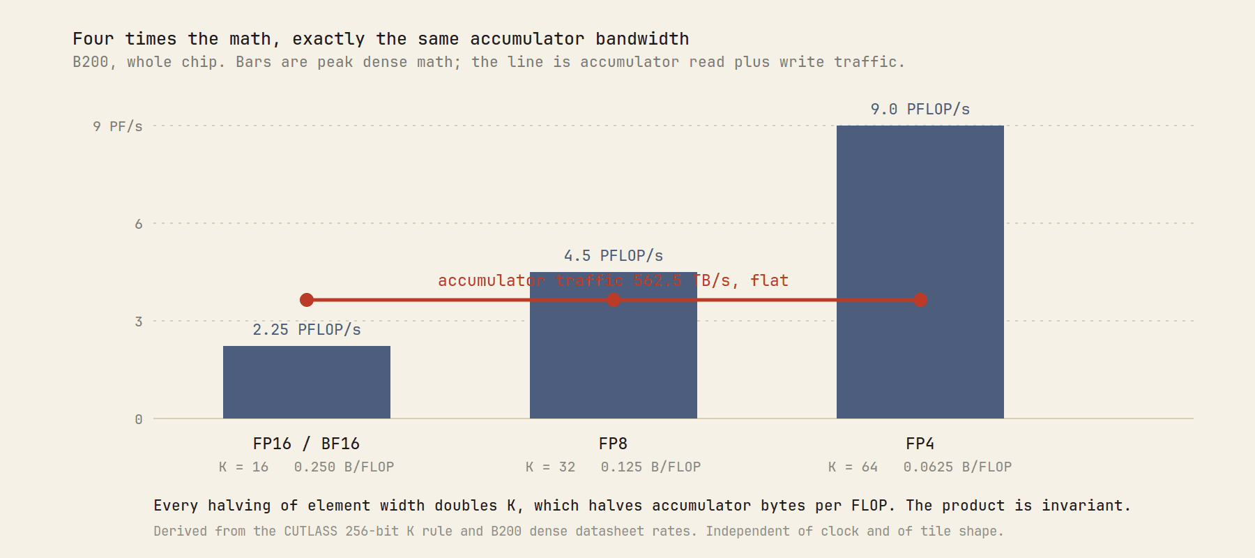
Figure 5. The invariance. This is the strongest single argument for why Tensor Memory is a fixed size, fixed geometry, precision-agnostic array: the bandwidth it must sustain does not depend on what numbers you put in it.
The other half, which explains where each operand lives
Run the same calculation on the inputs and the architecture stops looking like a set of choices and starts looking like a single constraint solved twice.
One UMMA reads an M by K slab of A and a K by N slab of B, so operand bytes are (M + N) times K times the element width, against the same 2MNK operations. The K cancels here too:
operand bytes per FLOP  =  (M+N)K b / (2MNK)  =  (M+N) b / (2MN)     // b = bytes per element

for the m128n256 tile:
FP16   b=2      0.01172 B/FLOP   x  2.25 PFLOP/s  =  26.4 TB/s
FP8    b=1      0.00586 B/FLOP   x  4.50 PFLOP/s  =  26.4 TB/s
FP4    b=0.5    0.00293 B/FLOP   x  9.00 PFLOP/s  =  26.4 TB/s

accumulator traffic / operand traffic  =  562.5 / 26.4  =  21.3 x
Invariant again, and for the same reason: halving the element width halves the operand bytes per FLOP at exactly the rate it doubles the FLOPs. So the precision ladder from FP16 down to FP4 is bandwidth neutral at both ends of the datapath.
Blackwell quadrupled its peak math without asking either the operand path or the accumulator path for one additional byte per second.
That is also the answer to a question the operand rules raise and never explain. Why must B sit in shared memory while D must sit somewhere else entirely? Because the accumulator moves twenty one times the traffic.
Operands are read once per instruction and are narrow by construction; the accumulator is read and written in full every single time, in FP32, no matter how few bits the inputs have. A general purpose memory can serve the first workload. Nothing general purpose serves the second.
It also explains a fact that otherwise looks like an oversight: Blackwell’s shared memory did not grow. 228 kilobytes per SM, identical to Hopper, in a generation that doubled math per SM per clock. It did not need to.
And where operand pressure did rise, NVIDIA answered with sharing rather than capacity: under cta_group::2 two SMs in a texture processing cluster consume the same operands for one logical tile, which halves the per-SM operand traffic instead of doubling the memory that carries it.
562.5 terabytes per second across the chip is seventy times the entire HBM bandwidth of a B200, and 3.8 terabytes per second per SM sustained. Neither a cache nor a register file survives that.
What survives is a small, banked array physically adjacent to the consumer, addressed in the coordinate system the datapath already uses, and free of every general purpose obligation: no coherence, no cache tags, no arbitrary indexing, no participation in the memory model, no ability to be read by an ALU.
Which is precisely the list of things TMEM cannot do. The restrictions are not a first generation compromise to be relaxed later. They are the reason the number is achievable.
It is worth putting our figure next to the one measurement that exists. The Delaware group reports roughly 16 terabytes per second of TMEM read bandwidth on a B200. That is about four times the sustained accumulator requirement we derive, which is the right shape of answer: a peak port figure with headroom for drains overlapping accumulation, not a number that contradicts ours.
We would rather show both than pretend they measure the same thing.
A caution about that paper’s peaksThe same paper reports achieved throughputs as percentages of theoretical peak: FP4 at 7,700 TFLOPS being 96.2 percent, FP16 at 1,929.6 being 96.5 percent. Those imply peaks of about 8,004 and 1,999 TFLOPS, where the B200 datasheet says 9,000 and 2,250 dense.
Both of their implied peaks are 11.1 percent below the datasheet, consistently, which is what you get from assuming a clock about 11 percent lower than the one the datasheet figures use. Their measurements are probably fine.
Their percentages are relative to a different baseline than NVIDIA’s, and should not be read as 96 percent of the number on the box.
Occupancy stops meaning what it meant
Occupancy is the oldest performance heuristic in CUDA: resident warps per SM, limited by registers and shared memory, more of them meaning more latency to hide.
On Blackwell tensor kernels it is close to useless, and the reason is that a resource nobody’s occupancy calculator models now binds before the ones it does.
Start with what NVIDIA documents for compute capability 10.0, in the Blackwell tuning guide.
Register file: 64 K 32-bit registers per SM, unchanged.
Maximum concurrent warps per SM: 64, unchanged since Volta.
Maximum thread blocks per SM: 32.
Shared memory capacity per SM: 228 kilobytes, the same as Hopper, with 227 addressable by a single block after CUDA’s 1 kilobyte reservation.
Combined L1, texture and shared memory: 256 kilobytes, also the same as Hopper.
Read that list again with the previous sections in mind. Across a generation that doubled tensor throughput per SM per clock, not one of the classical occupancy resources grew.
The only capacity Blackwell added to the SM is the 256 kilobytes of Tensor Memory, and Tensor Memory is the one resource with an allocation rule that quantizes hard.
Columns come in powers of two, minimum 32, from a pool of 512, and every column carries all 128 lanes. So the pool admits 16 concurrent allocations at the smallest legal size, 8 at 64 columns, 4 at 128, 2 at 256, and 1 if you take the whole thing. There is no middle. And 16, the best case, is already half the hardware ceiling of 32 blocks per SM.
The moment your tile needs more than the minimum allocation, which any tile worth issuing a UMMA for does, Tensor Memory is the binding constraint and nothing else is close.
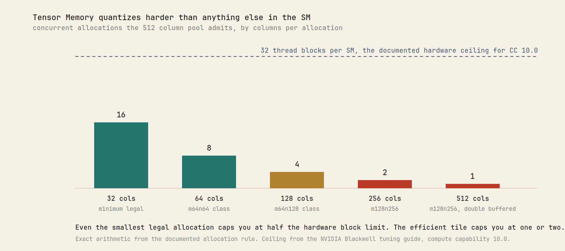
Figure 6. What the pool admits. This is an upper bound from the allocation rule, not a measurement of scheduler behaviour. Whether the hardware will actually co-resident that many CTAs is a separate question, and one we cannot settle without a B200.
That caveat is not decoration. Colfax’s post on the workstation part, contrasting it with the datacenter part, states flatly that on SM10x tcgen05.mma is locked to one CTA per SM. Colfax’s own tutorial kernel allocates all 512 columns for a single 128 by 256 tile and never revisits the question.
And the PTX manual describes tcgen05.relinquish_alloc_permit as a promise that the CTA will make no further allocations, which Colfax glosses as allowing future CTAs to queue up for the same SM. The word queue is doing a lot of work in that sentence.
It is consistent with a scheduler that admits a new CTA only when the pool can serve it, which would collapse figure 6 toward 1 for any realistic tile regardless of the arithmetic.
We cannot resolve that without hardware, and we would rather show the bound and name the uncertainty than assert a residency number we have not seen. What survives either reading is the shape of the problem: the resource that limits parallelism on a Blackwell SM is acquired at runtime, quantizes in powers of two, and does not appear in any static occupancy model.
Now the part that makes low occupancy survivable, which is the more interesting half.
What occupancy hid was memory latency: a warp stalls on a load, the scheduler runs another warp. In a Blackwell GEMM the loads are done by the Tensor Memory Accelerator, asynchronously, into shared memory, signalled by an mbarrier.
The math is done by a single elected thread issuing an asynchronous instruction that reads shared memory and writes Tensor Memory. Neither heavy operation is a thread stalling on anything. Latency is hidden by pipelining within one CTA, using barriers and multiple buffers, rather than by switching between CTAs.
The author writing as gau-nernst describes exactly this in a working kernel: multiple tcgen05.mma in flight, one mbarrier per stage, so different MMA stages can be waited on independently.
The Delaware measurements make the same point from the other side. Single instruction latency for tcgen05.mma is 11.0 to 11.4 clocks and nearly flat across tile shapes from m64n64k16 to m256n256k16. Hopper’s wgmma scales linearly with tile width, 32 clocks at m64n64k16 and 128 at m64n256k16.
A flat latency across a sixteen fold range of tile area is the signature of a spatial array, not a deeper pipeline.
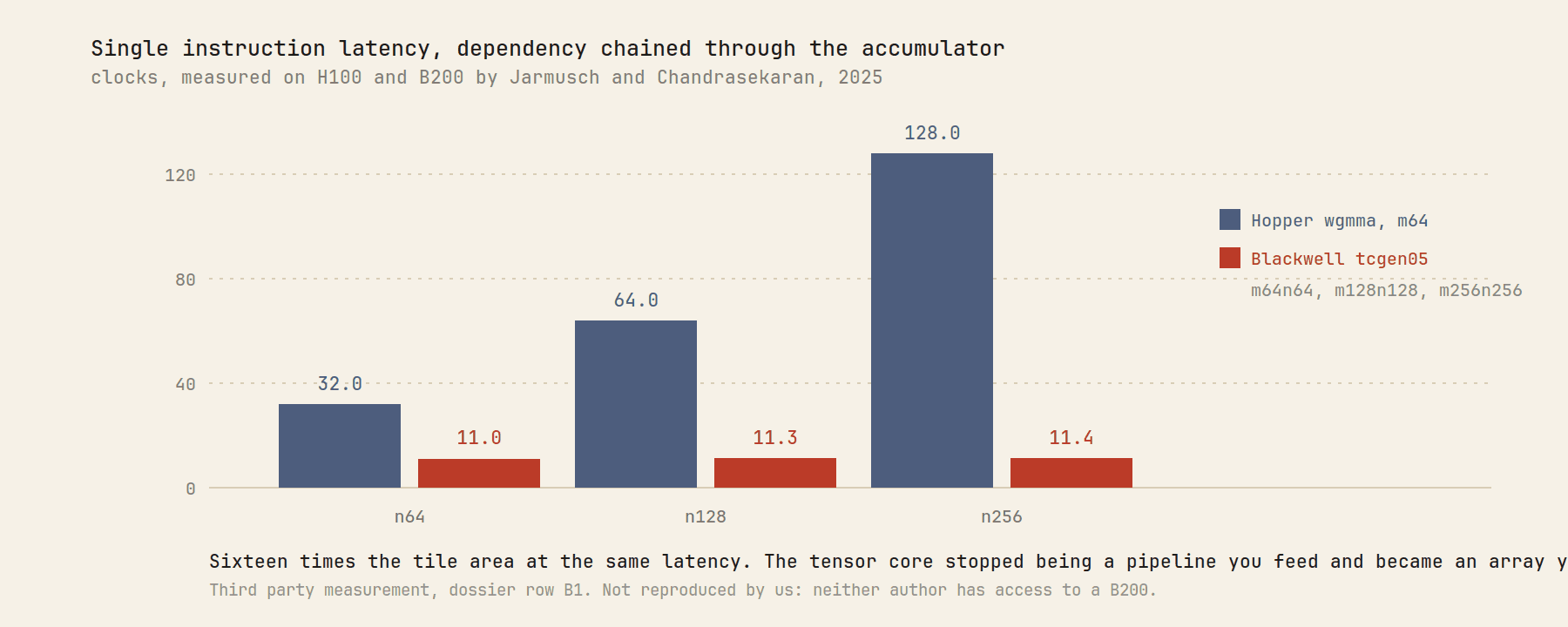
Figure 7. Hopper’s MMA latency grows with the tile. Blackwell’s does not. Combined with single thread issue and a TMEM resident accumulator, this is what makes very low CTA counts survivable.
So the tuning knobs invert. On Hopper you asked how many warpgroups fit and how to specialize them. On Blackwell you ask how many columns your accumulator needs, how many buffers fit in what remains, and whether the tile is worth a CTA pair.
The Nsight metric that used to matter, achieved occupancy, tells you almost nothing. The metric that matters has no counter.
Quantization became an allocation problem
Here is the part we think is genuinely underappreciated, and it is the point where this architecture stops being a matter for kernel authors and starts being a matter for anyone who chooses a serving format.
Blackwell implements block scaling in hardware. A block scaled MMA computes D = C + (A x SFA) times (B x SFB), where SFA and SFB are vectors of scale factors, one per group of 16 or 32 elements along K.
The scale factors are not folded in beforehand and they are not applied afterwards. They are consumed by the tensor core as it runs. And, per the PTX ISA, they are consumed from Tensor Memory.
My disassembly shows this directly. The block scaled variants take a third and fourth tmem[] operand:
// kind::mxf4nvf4.block_scale.scale_vec::4X, NVFP4 with block16 scaling
UTCOMMA.4X gdesc[UR14], gdesc[UR16], tmem[UR8], tmem[URZ], idesc[URZ], tmem[UR8], UPT ;

// kind::mxf4.block_scale.scale_vec::2X, MXFP4 with block32 scaling
UTCOMMA    gdesc[UR14], gdesc[UR16], tmem[UR8], tmem[URZ], idesc[URZ], tmem[UR8], UPT ;
Read the consequence carefully. Your choice of numerical format now consumes the same scarce, power of two, 32 column granular, 512 column per SM resource that your accumulator consumes.
Finer scaling is not just more metadata bandwidth from HBM. It is columns you cannot use for the accumulator, for double buffering, or for a second CTA.
The two formats differ exactly where it hurts. MXFP4 follows the Open Compute microscaling specification: blocks of 32, scale in E8M0, a bare power of two exponent.
NVFP4 is NVIDIA’s own: blocks of 16, scale in E4M3, a real floating point number with a mantissa, plus a second level FP32 tensor-wide scale. Per the PTX rules, block32 must pair with E8M0, while block16 may use E8M0 or E4M3.
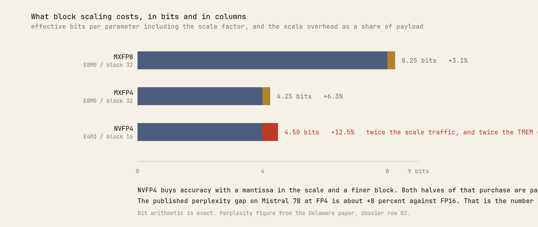
Figure 8 NVFP4 halves the block size and puts a mantissa in the scale, which is why it is more accurate than MXFP4. It also doubles the scale factor footprint, and that footprint lives in the same 512 column pool as the accumulator.
This is a co-design decision hiding inside a numerics decision. NVIDIA defined a format whose accuracy advantage over the open standard comes from finer blocks and richer scales, then built the only silicon where those scales are consumed directly out of a dedicated on-chip memory rather than being unpacked into registers first.
On hardware without that memory, the same format is a software dequantization problem with a register cost. On Blackwell it is an operand.
The Delaware group reports the accuracy side: FP8 costs about 2 percent perplexity on Mistral 7B and Mixtral 8x7B, FP4 costs 8 to 9 percent, and their FP4 throughput is 2.5 times FP16 on the dense model and 2.7 times on the mixture of experts model.
Whether 8 percent perplexity is acceptable is a per-layer question and always was. My point is narrower: on this architecture the answer is also a per-SM capacity planning question, because the scale factors and the accumulator compete for the same 512 columns.
Numerics stopped being a property of the model and became a property of the memory allocator.
What this does to serving economics
Everything above is architecture. Here is the part that shows up on an invoice.
Two rules from earlier sections collide here. The UMMA shape table offers exactly two values of M for a single CTA, 64 and 128; there is nothing smaller.
And allocation is by whole column, so the accumulator’s footprint is fixed by the tile you chose, not by the rows you filled.
During prefill neither rule bites. M is the token count of a chunk, thousands of rows, and the tile is full. During decode both bite at once. A decode step is a GEMM whose M is the number of sequences you are batching, and it is skinny by construction, so you pick the 64-row tile and leave most of it empty.
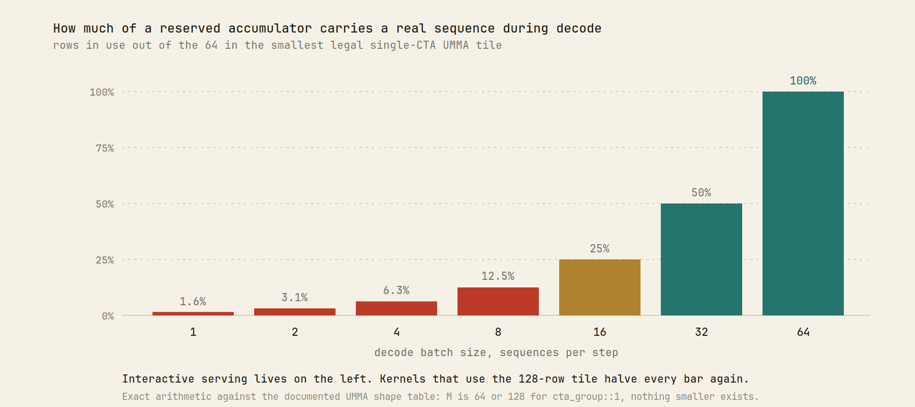
Figure 9 The decode penalty, stated against the most favourable tile the instruction set offers. At a batch of eight, an ordinary steady state for a latency sensitive endpoint, an eighth of the reserved accumulator carries anything. The rest is allocated, idle, and unavailable to any other block on that SM.
Be precise about what is and is not new, because it is easy to overstate. The 64-row floor is not new: Hopper’s wgmma had exactly the same minimum M, and skinny GEMMs have underused tensor cores since Volta.
That is why prefill and decode get disaggregated onto separately provisioned pools in the first place, which we argued at length in a previous issue.
What is new is where the waste is recorded. Previously it was purely a throughput loss: you issued an MMA whose M dimension was mostly zeros and you got a fraction of peak flops, and the moment the instruction retired the machine was free again.
Now the same tile also holds a capacity reservation, in a 512 column pool, acquired through an atomic that other CTAs may be spinning on, held for the tile’s lifetime, and invisible to every static occupancy model. Underutilisation stopped being a transient and became an allocation.
Three practical consequences follow, and we hold them with decreasing confidence.
The first is that Blackwell widens the gap between prefill and decode economics rather than narrowing it, in a generation whose marketing is entirely about inference. The FP4 tensor cores are a prefill and large-batch story, and section 05 is the reason: the precision ladder is bandwidth neutral on chip, so what FP4 buys you is math you can only spend if you have rows to fill. Decode has neither. It remains bound by HBM bandwidth for weight movement, and now carries an on-chip capacity reservation on top. This is consistent with the Delaware measurements from a different angle: as precision drops from FP16 to FP4 their measured memory bandwidth utilization falls from 67 percent to 48 percent, which is what it looks like when a workload stops being bandwidth bound and starts being bound by something else.
The second is that this pushes harder toward every technique that manufactures M. Speculative decoding turns one sequence into k candidate tokens per step, and on Blackwell it is not only amortizing weight reads across more rows, it is filling rows of a tile that was reserved whether or not you filled them.
Figure 9, read the other way, is a chart of how much accumulator a speculative draft gets for free. We modelled speculation as a throughput question in a previous issue. There is a second term in that model now, and it points the same way.
The third, and the one we are least sure of, is that grouped GEMM for mixture of experts becomes a harder allocation problem than it was. Each expert’s tile has its own M, determined by routing, varying per step. If your kernel allocates for the worst case it wastes columns on every expert that got fewer tokens; if it allocates per expert it pays the atomic repeatedly.
The one worklog we have found on optimizing NVFP4 grouped GEMM on Blackwell, by Mufeez Amjad, lands on cta_group::2 with a shared TMEM allocation across the CTA pair, and describes the shared allocation as one of the main benefits rather than the wider math tile. That is a hint about where the pressure actually is.
What Rubin says about whether this was a one-off
A reasonable objection to everything above is that Tensor Memory might be a Blackwell specific hack, a way to ship a doubled MMA without redesigning the register file, and that the next architecture folds it back into something more general.
NVIDIA published enough about Rubin on 21 July 2026 to answer that. It is not going away, and every disclosed change points at the numbers in section 05.
Three details in NVIDIA’s own post are load bearing.
Tensor Memory gained a consumer that is not the MMA. In the long context attention path, the intermediate scores from the dense QK transpose are, in NVIDIA’s words, loaded from Tensor Memory into a structured 2 to 4 sparse compressed form, generating both the nonzero values and the metadata. TMEM is no longer only where accumulators land. It is a staging tier that a hardware compression path reads from. That is the same direction our disassembly already showed on Blackwell, where sparsity metadata and block scale factors are already TMEM operands.
Rubin doubles the K dimension per tensor core instruction. NVIDIA frames this as fewer K loop iterations and less loop overhead, which is true and is the reason a reader would care. Run it through section 05 and it is also something else. Accumulator bytes per FLOP is 4 over K. Doubling K halves it. If Rubin’s NVFP4 K goes from 64 to 128, accumulator traffic per unit of math drops by half at exactly the moment the math rate goes up. That is the same invariance trick applied across a generation instead of across a precision ladder, and it is the strongest evidence we have that accumulator bandwidth is a first order design constraint at NVIDIA rather than a consequence.
Softmax became the bottleneck, so they widened it. Rubin raises exponential throughput per clock per SM by 2 times for FP32 and 4 times for BF16 against Blackwell, with Blackwell Ultra at 2 times for both. You only build that if the matrix path has already pulled far enough ahead that the transcendental path is what is left.
Alongside those, Rubin adds inline descriptor updates for the Tensor Memory Accelerator, so a mixture of experts kernel keeps one descriptor and overrides the pointer and stride fields in the instruction instead of rewriting a descriptor in memory per expert, and counted writes for device initiated NVLink transfers so the receiver tracks completion without the barrier, acknowledgement and atomic flag sequence.
Every one of those is the same move: take a coordination cost that was paid in general purpose instructions and registers, and pay it in a dedicated mechanism instead. Tensor Memory was the first large instance. Rubin is the pattern applied to descriptors, to synchronization, to sparsity metadata and to the softmax path.
One sentence for what NVIDIA is doing to the SM across these two generations: they are disassembling the general purpose core into special purpose engines connected by dedicated memories and barriers, and leaving the threads to do bookkeeping.
The execution model is being hollowed out from the inside while its surface syntax stays the same.
Where this could be wrong
The accumulator traffic derivation assumes a full read and write per instruction. If the tensor core retains partial accumulator state internally across the K extent, or streams only the sub-tile currently in flight, then 562.5 terabytes per second is an upper bound. What makes us reasonably confident is not the absolute number but the invariance: the cancellation between element width and K is exact, holds at three precisions, and falls out of a rule visible in CUTLASS source. A different traffic model would change the constant and probably not the invariance. Note that this is a revision of an earlier draft of ours, which held K fixed at 16 across precisions and therefore produced a per-SM figure four times too large at FP4.
We are reading the SASS of a probe, not of a real kernel. A kernel with one MMA gives
ptxasno scheduling problem to solve. The allocation spin loop may be scheduled very differently, hoisted, or dominated by something else in a CUTLASS mainloop with a producer warpgroup and four pipeline stages. We are confident the instruction sequence exists and that the guardrails are unconditional. We are not confident about its cost in situ, and the 152 instruction figure is a property of our probe, not of production kernels.Figure 6 is an upper bound, not a residency measurement. The allocation arithmetic is exact, and the documented block and warp ceilings for compute capability 10.0 are exact. What we cannot verify is whether the scheduler will actually co-resident the CTAs the pool arithmetically admits. One published source states that SM10x is locked to one CTA per SM outright, and the PTX description of
relinquish_alloc_permithints at queueing rather than co-residency. If that reading is right, the correct version of figure 6 is a flat line at 1, the argument gets stronger rather than weaker, and our chart is still wrong.Figure 9 measures reservation, not throughput, and only for the tile we chose. The 64 row floor is documented and the arithmetic against it is exact, but a real decode kernel may prefer a different shape, may reuse one allocation across many tiles, or may batch several matrices into a single call in ways that change what fraction of the pool sits idle at any instant. The claim we will defend is narrow: below 64 sequences the accumulator is reserved for rows that do not exist. What that costs in dollars depends on a serving stack we have not profiled.
The Blackwell per-SM per-clock figure of 8,192 is inferred, not published. Volta, Ampere and Hopper rates come from NVIDIA whitepapers and reproduce the published teraflops to three digits. For Blackwell we ran the identity backwards from 2.25 petaflops over 148 SMs, which requires 8,192 FLOPs per clock at 1.86 GHz. If the real SM count in the shipping part differs, or if the datasheet figure assumes a different clock, the doubling claim survives but the exact number moves.
The portability finding is solid; the moat reading of it is not. Section 04 already discounts it and we would discount it further rather than less. The instruction family genuinely does not exist outside datacenter Blackwell. What follows from that commercially is much weaker than it first sounds.
Four predictions, each with its failure condition
Deliberately conservative, and each one checkable by a specific date against a specific artifact.
NVIDIA will not expose Tensor Memory to a general purpose instruction through the end of 2028. No
ld,st, atomic or ALU operand outside thetcgen05family, in Rubin or its successor. The invariance in section 05 is the reason: general purpose addressability is incompatible with the bandwidth. Wrong if a PTX ISA revision adds any TMEM access outside the dedicated opcode family.By 31 December 2027, no open source compiler will generate a
tcgen05GEMM within 10 percent of CUTLASS on a mainstream shape without hand written PTX in its lowering path. Reaching the instruction is already happening. Reaching it through a general lowering that models column allocation, the warp-lane access partition and the drain width tradeoff is a different problem. Wrong if a mainline release of Triton, Mojo or tinygrad hits the bar with a pure compiler path.Nsight Compute will ship a Tensor Memory occupancy or column pressure section before the end of 2028. The hardware is already tracking the pool, since the allocator does a find-and-set against it, and there is currently no static way to reason about a resource acquired at runtime. Wrong if no NVIDIA profiler release by then reports TMEM allocation state.
NVFP4 will remain the default four bit format in NVIDIA’s own inference libraries through 2027, and MXFP4 will not displace it there. Not an accuracy argument: the block16 path is the one with a dedicated opcode modifier and a hardware operand path on the silicon that matters. Wrong if TensorRT-LLM or NVIDIA’s quantization tooling defaults to block32 for four bit weights.
We have dropped two predictions that appeared in an earlier draft, on model architectures being shaped around column boundaries and on serving share ratios between formats, because neither had a failure condition we could actually check.
Confidence dossier
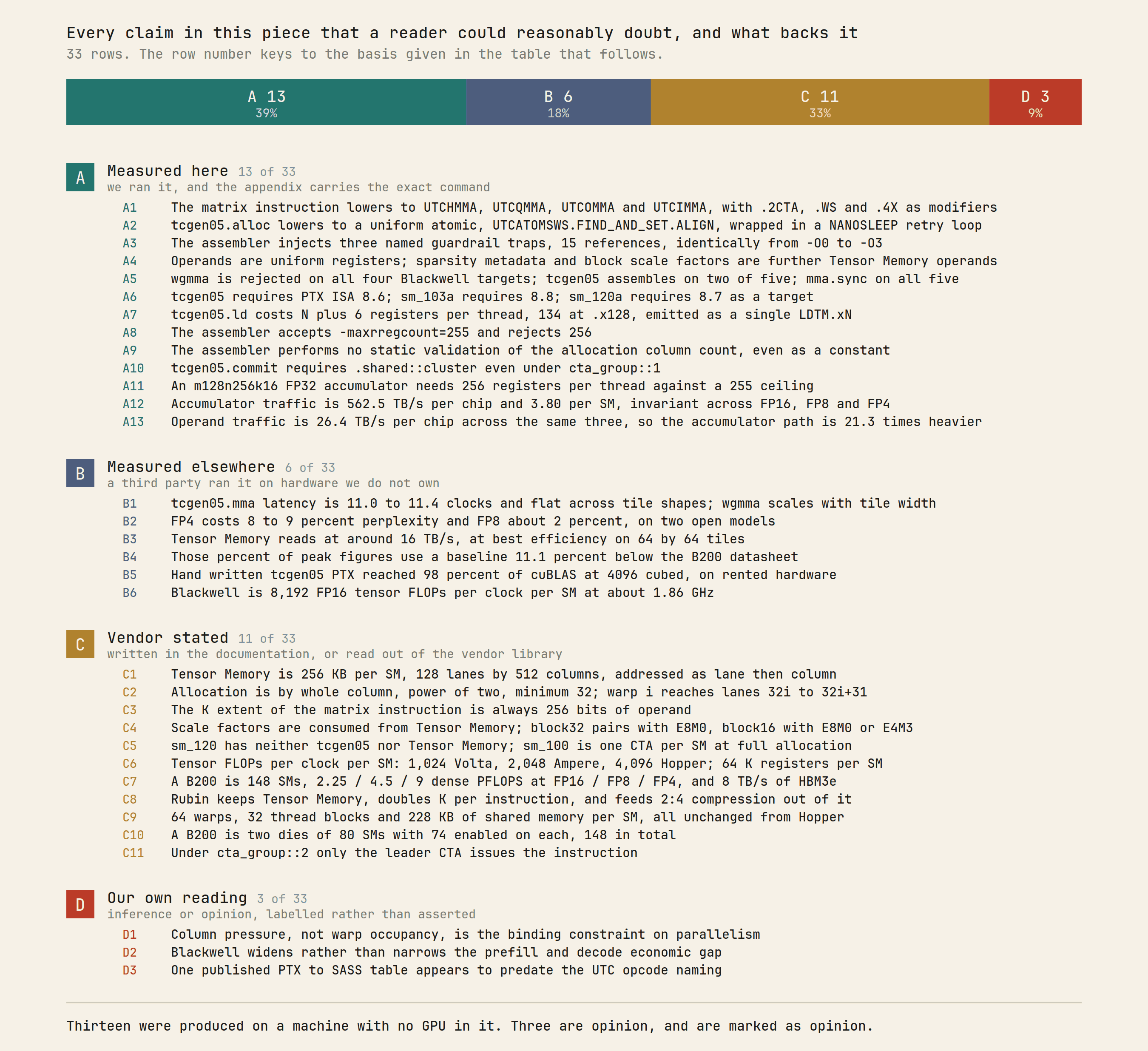
Reproduce every tier A row on a machine with no GPU
Everything in tier A came out of the following, in a clean container, in under five minutes, with no CUDA installation and no driver.
# 1. the toolchain, as ordinary x86 binaries from PyPI
pip download nvidia-cuda-nvcc-cu12 --no-deps -d /tmp/w            # ptxas 12.9.86
pip download nvidia-cuda-nvdisasm nvidia-cuda-cuobjdump --no-deps -d /tmp/w   # 13.3.73
mkdir -p /tmp/tk && cd /tmp/tk && for f in /tmp/w/*.whl; do unzip -oq "$f"; done
PTXAS=/tmp/tk/nvidia/cuda_nvcc/bin/ptxas
DIS=/tmp/tk/nvidia/cu13/bin/nvdisasm

# A1, A2, A3, A4: assemble the probe and read the machine code
$PTXAS -arch=sm_100a probe.ptx -o probe.cubin && $DIS -c probe.cubin | less
$DIS -c probe.cubin | grep -oE '__cuda_sm10x_tcgen05_[a-z_]+' | sort -u
for o in 0 1 2 3; do $PTXAS -O$o -arch=sm_100a probe.ptx -o g.cubin
  echo "-O$o $($DIS -c g.cubin | grep -c guardrail) refs, \
$($DIS -c g.cubin | grep -cE '^\s+/\*[0-9a-f]{4}\*/') instructions"; done

# A1 continued: one build per .kind qualifier
for k in f16 tf32 f8f6f4 i8; do sed "s/kind::f16/kind::$k/" probe.ptx > k.ptx
  $PTXAS -arch=sm_100a k.ptx -o k.cubin && $DIS -c k.cubin | grep -oE 'UTC[A-Z0-9.]+'; done

# A5: three instruction families across five targets
for a in sm_90a sm_100a sm_103a sm_100 sm_120a; do
  for f in probe legacy_wgmma legacy_mmasync; do
    printf '%-9s %-16s ' $a $f; $PTXAS -arch=$a $f.ptx -o /dev/null 2>&1 | head -1; echo; done; done

# A6: minimum PTX ISA version
for v in 8.3 8.4 8.5 8.6 8.7 8.8; do sed "s/^.version 8.6/.version $v/" probe.ptx > v.ptx
  echo -n "$v "; $PTXAS -arch=sm_100a v.ptx -o /dev/null 2>&1 | head -1; echo; done

# A7: the epilogue register curve. widen tcgen05.ld to .xN and store every register
for n in 1 2 4 8 16 32 64 128; do $PTXAS -arch=sm_100a -v ld_$n.ptx -o /dev/null 2>&1 | grep Used; done

# A8, A9: the ceilings the compiler will and will not enforce
$PTXAS -arch=sm_100a -maxrregcount=256 probe.ptx -o /dev/null
for c in 16 48 96 1024; do sed "s/mov.u32 %r1, 128;/mov.u32 %r1, $c;/" probe.ptx > a.ptx
  $PTXAS -arch=sm_100a a.ptx -o /dev/null && echo "$c columns: accepted"; done
Two practical notes. ptxas from the 12.9 wheel caps at PTX ISA 8.8, which covers sm_103a and nothing above it, so pull a newer nvidia-cuda-nvcc for later targets. And nvdisasm from the CUDA 13 wheels reads CUDA 12 cubins, which is convenient because the CUDA 13 nvcc wheel did not build in our container while the standalone disassembler wheels did.
The value of this workflow is not that it replaces a GPU. It is that it separates two questions that get conflated constantly in GPU writing: what the machine does, which needs hardware, and what the compiler emits, which does not.
A surprising share of public claims about the CUDA moat are claims of the second kind, and the second kind is checkable by anyone with forty megabytes of disk.
Bibliography
NVIDIA, Parallel Thread Execution ISA: tensor memory addressing, tcgen05 MMA and its kind shapes, shared memory descriptors, instruction descriptors, data path layout organization, and the tcgen05 memory consistency model. The primary source for everything structural here.
NVIDIA, Blackwell Tuning Guide and Ampere Tuning Guide. Register file size, the register per thread ceiling, warp and thread block limits per SM, and shared memory capacities for compute capabilities 8.0, 10.0 and 12.0.
NVIDIA Volta, Ampere and Hopper architecture whitepapers. Source for 1,024, 2,048 and 4,096 FP16 tensor FLOPs per clock per SM, each of which reproduces the corresponding published teraflops figure to three digits.
NVIDIA, HGX B200 datasheet. Dense and sparse rates per precision, with the explicit note that dense is half of sparse, plus memory capacity and bandwidth.
Ryo, CUTLASS Tutorial: Writing GEMM Kernels Using Tensor Memory For NVIDIA Blackwell GPUs, Colfax Research, April 2025, updated November 2025. The clearest published account of TMEM allocation, UMMA operand rules and the CuTe abstractions over both.
Colfax Research, CUTLASS Tutorial: Hardware-supported Block-scaling with NVIDIA Blackwell GPUs. Scale vector rules and TMEM layouts of scale factors.
Colfax Research, NVFP4 Blockscaled GEMM on NVIDIA RTX Pro Blackwell GPUs (SM12x), June 2026. The explicit statement that SM12x has neither tcgen05 nor TMEM, and that SM10x is locked to one CTA per SM.
NVIDIA, CUTLASS source,
include/cute/atom/mma_traits_sm100.hppandcopy_traits_sm100.hpp. The 256 bit K rule, the TMEM copy atoms, and the ThrID change.Aaron Jarmusch and Sunita Chandrasekaran, University of Delaware, Microbenchmarking NVIDIA’s Blackwell Architecture: An in-depth Architectural Analysis, arXiv 2512.02189. The only systematic public measurement of B200 tensor core latency, TMEM behaviour and FP4 accuracy we are aware of.
NVIDIA, Inside NVIDIA Rubin GPU Architecture: Powering the Era of Agentic AI, 21 July 2026.
NVIDIA, CUTLASS documentation, Blackwell SM100 functionality. The seven tcgen05.mma instructions and the block scaled data types.
SemiAnalysis, Dissecting NVIDIA Blackwell: Tensor Cores, PTX Instructions, SASS, Floorsweep, Yield. The CuTe ThrID observation and the TPC scoped CTA pair framing.
gau-nernst, tcgen05 for dummies, December 2025. A working tutorial in plain CUDA and inline PTX.
Mufeez Amjad, Optimizing NVFP4 Grouped GEMM on Blackwell, worklog, March 2026. The CTA pair and shared TMEM allocation observation in section 08.
Rouhani et al., Microscaling Data Formats for Deep Learning, arXiv 2310.10537. The MX specification behind MXFP4 and MXFP8.
NVIDIA developer forums, thread on computing tensor core FP16 throughput per SM per clock from whitepaper figures. The identity used in section 01.
Chips and Cheese, Nvidia’s B200: Keeping the CUDA Juggernaut Rolling, December 2025. Die level SM counts: 74 enabled of 80 per die.
Austin et al., How To Scale Your Model, GPU chapter. Independent derivation of Blackwell’s per-SM per-clock tensor rate from the same datasheet figures.
Our own previous work: How the NVIDIA Compiler Moat Actually Works, How CUDA Binaries Actually Work, The Split and the Seam on prefill and decode disaggregation, and The Draft and the Ledger on speculative decoding economics.