



Introduction
I’ve never had a MI300X in front of me. I’m perfectly aware that’s the wrong way to start a piece about ROCm, but it’s also the exact same reason this one needs to exists.
Every time I’ve tried to read seriously about AMD’s software stack I have hit the same wall: the writing is either marketing, or it is a benchmark table, or it is a bring-up worklog by someone who rented eight cards for a week and is understandably more interested in getting a model to run than in explaining what the machine is.
What I wanted was the thing I’d want for any other system I do not own: a description precise enough that I could predict what it would do.
You can get closer to that than you would think without hardware, because of a property of ROCm nobody right now seems to exploit. The stack is open down to the instruction encodings, the compiler that targets it is upstream LLVM, and the compiler is an x86 program.
Everything here was produced on a single-core container with no GPU attached: clang 20.1.2 and 22.1.0 from the official builds, and about three hundred megabytes of YAML cloned out of a public AMD repository.
I just compiled real code objects for five AMD datacenter targets, decoded their kernel descriptors byte by byte, and counted the entire shipped tuning surface of AMD’s GEMM library.
One result surprised me a lot. From gfx90a to gfx942, every matrix instruction AMD had carried forward. In the case of gfx942 to gfx950, every single one carried forward again.
Then, from gfx950 to gfx1250, the compute die inside the MI455X that AMD launched into the Helios rack in July, the number that carries forward is zero.
I repeat: it’s not reduced to a numbr near zero. It’s just zero of seventy five, and the wavefront changes width at the same time. Most of this piece is about the context needed to say why that matters and what it does not mean, because the obvious reading is wrong in an interesting way.
The second thing is smaller but I think it’s more durable. AMD’s openness has been taken as a virtuous example for a decade, as though the interesting question were whether a stack is open. The interesting question is what openness lets you count.
Here it lets you count the kernel layer exactly: 16,177 generated assembly kernels and 2,905,048 measured mappings from problem shape to kernel, in a git repository anyone can clone.
There is no counterpart on the other side. NVIDIA’s equivalent is not secret so much as uncountable, because there is no file.
What ROCm is, in the order the electrons see it
In my personal findings, I kept seeing that the word ROCm is used for at least three different things: a kernel driver, a runtime and compiler toolchain, and a large collection of libraries that happen to be distributed together.
Talking about “ROCm performance” without saying which of the three you mean is how most arguments about AMD software go wrong. Here is the stack, bottom to top, with the piece of the problem each layer owns.
At the bottom we see
amdgpu, the kernel driver, which has been in the mainline Linux tree since 2015 and is the same driver that runs a gaming Radeon. Inside it lives the KFD, the compute component, which owns the queues, the doorbells, the page tables and the notion of a process having a GPU address space.Above it in user space sits libhsakmt, historically called the Thunk, a thin ioctl wrapper, and above that ROCr, the HSA runtime, which implements a specification written by a foundation AMD co-founded in 2012 for a world that never quite arrived, and which left behind an unusually well documented dispatch model.
On top of ROCr sits HIP, which is two things wearing one name. HIP, the language, is a near copy of CUDA C++ with the identifiers renamed. HIP the runtime is a library exposing an API that is a near copy of the CUDA driver and runtime APIs with the identifiers renamed. The compiler is not a fork of anything proprietary; it is clang, with a device-side target of
amdgcn-amd-amdhsa, plus a bitcode library of device functions called ROCm Device Libs where the math lives.Above HIP sit the libraries, and this is where most of the engineering hours are: rocBLAS and hipBLASLt for GEMM, MIOpen for convolutions and some fused primitives, Composable Kernel as a template layer for writing fused operators, RCCL for collectives, and since 2025 AITER, which is AMD’s answer to the observation that a serving engine does not want a BLAS, it wants attention and mixture-of-experts kernels.
Above that sit the frameworks, and above those the serving engines, vLLM and SGLang, which is where a customer’s dollar actually meets the machine.
Ten layers, counted that way. For any performance claim about AMD, the useful question is which layer it is a claim about, because they differ wildly in maturity and in rate of change.
The driver is boring and solid, and the runtime is the same. The compiler is upstream LLVM and is very good. The library layer is where the variance lives, and the variance is enormous.
The dispatch packet is a struct, and you can read it
Start with the thing that is most unusual about ROCm, because it sets up everything else.
When a CUDA program launches a kernel, nobody truly knows what happens between <<<>>> and the SM starting work. There is a channel, there is a doorbell, there is a scheduler; the formats are entirely IP and the only supported way to produce them is to call NVIDIA’s runtime.
On AMD, kernel dispatch is a 64 byte structure whose every field is in a published specification, written by user space into a ring buffer that user space allocated, and signalled by a store to a doorbell page that the driver mapped into the process.
The structure is the AQL kernel dispatch packet. It carries a header with the packet type and two memory fence scopes, the workgroup dimensions and grid dimensions as three 16 bit and three 32 bit fields, the sizes of the private and group segments, a pointer to the kernel object, a pointer to the kernarg buffer, and a completion signal handle.
A queue is a ring of these packets plus a read index and a write index. Submitting work is: write the packet, bump the write index, store to the doorbell.
Two fields in that structure carry most of the interesting behaviour. The barrier bit, when set, says that this packet may not begin until every preceding packet in the same queue has completed, which is what makes an HSA queue behave like a CUDA stream.
The two fence scope fields say what memory ordering the hardware must establish at packet start and packet end, with values for no fence, agent scope, and system scope. Those two fields are the reason a stream on AMD has an ordering cost that is visible and adjustable rather than implicit.
The practical consequence is a line buried in AMD’s tuning documentation recommending GPU_MAX_HW_QUEUES=2, with the note that hardware efficiency is maximised at four or fewer HIP streams.
A HIP stream is not free the way an abstraction is free: it maps to a hardware queue, which are a finite resource arbitrated by the command processor, and oversubscribing them makes the scheduler do work that surfaces as launch latency.
The same document says plainly that ROCm serialises kernel launches across GPUs from one process, which is why RCCL wants one process per GPU. Elsewhere these would be folklore. Here they are consequences of a dispatch model you can read.
Anatomy of an AMD code object
Now let’s compile something. This is a single MFMA loop, written in C with clang’s AMDGPU builtins, with no ROCm installation anywhere on the machine:
typedef float    f32x16 __attribute__((ext_vector_type(16)));
typedef _Float16 f16x4  __attribute__((ext_vector_type(4)));
#define G __attribute__((address_space(1)))

__attribute__((amdgpu_kernel))
__attribute__((amdgpu_flat_work_group_size(256,256)))
void gemm_tile(G f32x16 *out, G f16x4 *a, G f16x4 *b, int n) {
  f32x16 acc = (f32x16)(0.0f);
  for (int k = 0; k < n; ++k)
    acc = __builtin_amdgcn_mfma_f32_32x32x8f16(a[k], b[k], acc, 0, 0, 0);
  out[0] = acc;
}
clang --target=amdgcn-amd-amdhsa -mcpu=gfx942 -O3 -nogpulib \
-fuse-ld=lld -o ko_gfx942.hsaco ko.cThat produces exactly 4,848 bytes. What it creates is an ELF64 shared object, and not a container format, not a fat binary with a vendor magic number at the front; it’s a shared object, with OS/ABI: AMDGPU_HSA, Machine: EM_AMDGPU, fifteen sections and thirteen symbols, which llvm-readobj and readelf parse without being told anything special.
The target identity lives in the ELF header flags, and this is the first place the AMD and NVIDIA philosophies visibly diverge:
Flags [ (0x54C)
  EF_AMDGPU_FEATURE_SRAMECC_ANY_V4 (0x400)
  EF_AMDGPU_FEATURE_XNACK_ANY_V4   (0x100)
  EF_AMDGPU_MACH_AMDGCN_GFX942     (0x04C)
]
Three orthogonal things are encoded there. The machine, gfx942, is the ISA. XNACK is whether the code was built to tolerate page faults and retry memory operations, which matters for unified memory.
SRAMECC is whether the code was built for a part with ECC on the on-chip SRAM, which costs registers. Each has three states: on, off, and any, where any means the object is compatible with either setting of the machine it lands on.
Now, let’s try with our means to compare with what I found when I looked at NVIDIA’s side of this in my earlier work. There, architecture-specific features are folded into the target name itself, which is how you get sm_90a and sm_100a, and a target with the a suffix is not forward compatible in the way plain PTX is.
AMD’s scheme is basically the same problem solved by making the feature axis explicit and orthogonal to the ISA version, with a documented neutral value.
Generally speaking, we’re looking at a better design, and it is worth saying that clearly because it’s one of the places where the open stack is not merely as good as the closed one, but it’s an order of magnitude better.
Inside the object, each kernel has two symbols: the code, and a 64 byte kernel descriptor in .rodata named <kernel>.kd. The descriptor is what the command processor reads to set up a wave.
Here is the one clang emitted for gfx942, byte for byte, and decoded:
00 00 00 00 00 00 00 00  1c 00 00 00 00 00 00 00
40 11 00 00 00 00 00 00  00 00 00 00 00 00 00 00
00 00 00 00 00 00 00 00  00 00 00 00 82 00 af 00
84 00 00 00 08 00 00 00  00 00 00 00 00 00 00 00

group_segment_fixed_size   = 0
private_segment_fixed_size = 0
kernarg_size               = 28
kernel_code_entry_offset   = 4416
compute_pgm_rsrc1          = 0x00af0082
compute_pgm_rsrc2          = 0x00000084
compute_pgm_rsrc3          = 0x00000000
kernel_code_properties     = 0x0008
kernarg_preload            = 0x0000
The rsrc words are hardware register images. rsrc1 bits 5:0 hold the granulated VGPR count, which is 2 here, meaning an allocation of 24 registers for a kernel that uses 20, because the encoding granule on this part is eight.
Bits 9:6 hold the granulated SGPR count. Bits 17:16 and 19:18 hold the denormal mode for 32 bit and for 16 and 64 bit floats independently, both set to 3 here, meaning flush nothing. Bit 23 is IEEE mode.
rsrc2 bits 7, 8 and 9 enable the workgroup id in SGPRs per dimension, and bits 12:11 say how many workitem id dimensions arrive in VGPR0 through VGPR2. rsrc3 bits 5:0 are ACCUM_OFFSET, the register number where the accumulator half of the file begins, and bit 16 is TG_SPLIT.
Here the field is 0, so AGPRs start at register 4, and the metadata agrees: 20 registers total of which 16 are AGPRs. Four architectural registers for addresses, sixteen for the accumulator, and a descriptor field that says where the boundary is.
That descriptor is the complete contract between compiler and hardware scheduler for how a wave is configured. It is documented, stable, byte-addressable, and I read it with a general purpose ELF tool. The corresponding structure exists on the other side of the market, but you meet it, if at all, through a disassembler the vendor ships.
For anyone building tooling, a profiler or a binary rewriter or a security scanner, that difference is the whole project. On AMD those are ordinary programs.
Three targets, one source. The code objects are all 4,848 bytes with 1,472 bytes of .text, and the text differs between gfx90a and gfx942 in 113 of those bytes, and between gfx942 and gfx950 in 33.
That is what an incremental ISA revision looks like from the outside: the same program, the same schedule, a small number of re-encoded opcodes.
The hazard contract, which is the whole argument in miniature
Here is the thing I keep coming back to, because it is the most clear statement of what is actually different between the two stacks, and almost nobody frames it this way.
On modern NVIDIA hardware, the dependency interlock for fixed-latency instructions is not in the silicon. It is in a control field that the assembler writes into each instruction, and getting it wrong produces wrong answers rather than slow ones.
That makes the assembler correctness-critical, and it makes the assembler’s closure a consequence of an architectural choice about where to spend area and energy, not a policy anyone can simply reverse.
AMD made the opposite choice, and it is visible in every kernel the compiler emits. Waiting is an instruction. s_waitcnt takes counters, vmcnt for vector memory, lgkmcnt for LDS and scalar and message traffic, expcnt for exports, and the operand says how many outstanding operations of that class you are willing to leave in flight.
If you write s_waitcnt vmcnt(0) you have waited for all of them; vmcnt(1) means you will proceed with one still outstanding. In my MFMA loop the compiler emits exactly two distinct forms:
s_waitcnt lgkmcnt(0)
s_nop 4
The s_nop is the second half of the contract.
Matrix instructions on CDNA have structural hazards with specific, published cycle counts: after an MFMA writes an accumulator, a certain number of cycles must pass before particular kinds of reader can touch it, and if the compiler cannot fill those slots with useful work it must fill them with nothing, explicitly, by emitting a no-op with a repeat count.
LLVM has a whole pass for this, the hazard recogniser, and its rules are in the source tree.
So both vendors moved hazard management out of hardware and into software. That is the shared fact, and it is a much more interesting one than “AMD is open”.
The difference is where in software. NVIDIA put it in a field inside the instruction word, written by a program you cannot read, which means the hazard model is enforced by a compiler.
AMD put it in separate architectural instructions, in a published ISA, which means the hazard model is enforced by the program text itself and anybody can write it.
Follow that difference to its economic conclusion and you get something non-obvious. Because AMD’s hazard model is expressible, hand-written assembly is a viable production strategy on AMD in a way it is not on NVIDIA. And AMD uses it.
The GEMM library’s kernels are generated assembly. AITER’s fastest attention paths are hand-written assembly. This is not a stopgap; it is the design. The openness did not remove the labour of getting near the metal.
It moved the labour from a compiler team to a kernel team, and made it possible to do that work outside AMD, which is a real and underrated property. What it did not do is make the work smaller.
That is the shape of the whole argument, and the rest of this piece is an attempt to put numbers on it.
Waves, SIMDs, and why 64 is not 32 twice
One more piece of groundwork, because it is the most common source of wrong intuitions when a CUDA programmer reads AMD code.
A CDNA compute unit has four SIMD units, each sixteen lanes wide, and a wavefront is 64 work items. So one wavefront instruction occupies its SIMD for four cycles, which is the classic GCN cadence, and the natural unit of divergence is 64 rather than 32. Every lane mask is a 64 bit value in a pair of scalar registers.
The consequences propagate a long way up. A CUDA warp shuffle moves data among 32 lanes; the AMD equivalents, ds_bpermute_b32 and the DPP and permlane families, work across 64 and do not map one to one.
A reduction written for warp size 32 does not become correct by changing a constant. A kernel assuming __activemask() returns 32 bits is assuming a fact about hardware, not about the language.
Alongside the vector units sits a fully separate scalar unit with its own register file and cache, and AMD code is full of scalar instructions doing address arithmetic, loop control and uniform values that on NVIDIA occupy vector registers.
That is a slight advantage and the reason the register pressure story differs: uniform work has somewhere else to live.
On gfx1250 the wave becomes 32 wide, the compute unit becomes a workgroup processor in the RDNA style, and the scalar unit’s role changes. We will get there.
Four ways to touch memory, and why the ugly one wins
A CDNA kernel can address memory through four instruction families, and which one the compiler picks is among the larger performance levers in the stack.
It’s also where reading AMD assembly diverges most from reading NVIDIA assembly, and where a CUDA programmer’s instincts mislead.
The flat_ family takes a 64 bit address in a pair of vector registers and works out from the address whether it means global memory, LDS or scratch. Convenient and expensive: two registers per lane, plus an aperture check.
The global_ family takes the same 64 bit address but promises it is global, dropping the check and keeping the two registers. The ds_ family addresses LDS with a 32 bit offset and is the only way to touch the scratchpad.
Then the buffer_ family, which is the interesting one. A buffer instruction takes a resource descriptor of four scalar registers holding a base address, a byte count, a stride and some format fields, plus a 32 bit offset per lane.
The descriptor lives in scalar registers, shared by all 64 lanes at a cost of zero vector registers, and the byte count means that the hardware does the bounds check: an access past the end returns zero for loads and discards stores, with no branch.
So a buffer_load_dwordx4 needs one vector register for the offset where a global_load_dwordx4 needs two for the address. On a kernel with a dozen live pointers into a tile that is a dozen registers per lane, in an architecture whose currency is registers.
The free bounds check is worth more still, deleting the masking and predication a tiled GEMM epilogue needs for its ragged edges.
Hence AMD’s tuning advice preferring buffer_load, Triton’s AMD backend having a pass that converts pointer arithmetic into buffer operations when it can prove the offsets fit in 32 bits, and hand-written AMD kernels being full of them.
It is an idea that is simply better than the alternative and that nobody outside the AMD world discusses, because the alternative is what everyone learned first.
The instruction that AMD’s own guide singles out as the one that moved a reference GEMM by sixty percent is in this family: buffer_load_to_lds, which reads global memory and writes LDS without the data ever entering a register.
Thats the same idea as NVIDIA’s asynchronous copy, just from a different angle, and its value is measured in registers returned to the accumulator rather than in latency hidden.
The wait counters, in detail
I said earlier that waiting is an instruction. It is worth being precise about what the counters count, because the semantics are unusual and they explain a class of AMD performance bug that looks like nothing on a profile.
Three counters are visible to a wave. vmcnt counts outstanding vector memory operations. lgkmcnt counts a grab bag: LDS, GDS, scalar memory reads and messages. expcnt counts exports and matters mostly for graphics.
The crucial property is that vmcnt returns in order and lgkmcnt does not. Vector memory completes in issue order, which is what makes s_waitcnt vmcnt(3) meaningful: three loads may still be in flight and you know exactly which three.
Scalar memory inside lgkmcnt can complete out of order, which is why you almost always see lgkmcnt(0) and almost never a nonzero value where scalar loads are involved. The compiler is not being lazy; it cannot express the thing you want.
That shapes how a software pipeline is written here. Prefetch depth is fine grained on the vector path and all or nothing on the scalar one, so AMD kernels push everything they can into vector memory even when the data is uniform, and reserve the scalar path for values consumed once at the top of a loop.
It also explains a specific pathology: mix LDS traffic and scalar loads inside a loop and every s_waitcnt lgkmcnt(0) for an LDS dependency drains the scalar loads too, needed or not. Hoisting them out fixes it, and the reason it works is a counter aliasing decision made a decade ago.
Occupancy, computed rather than guessed
Occupancy on AMD is arithmetic you can do on paper, and AMD publishes the formula, which is not something you can say about every vendor.
Each SIMD has 512 VGPRs available to it in wave64 terms, allocated to waves in blocks of sixteen. That is a different quantity from the granule of eight in the kernel descriptor: eight is how the count is encoded, sixteen is how the hardware hands registers out.
So a kernel using 170 registers is rounded to 176, and the number of waves that fit per SIMD is the floor of 512 over 176, which is two, because three times 176 is 528 and that does not fit. If you can push the kernel to 168 registers you get three waves, a fifty percent increase in latency hiding, for a change of two registers.
This is the entire reason waves_per_eu exists as a Triton parameter: it is a hint to the register allocator to try harder to land under a threshold that the programmer can compute and the allocator does not know about.
The workgroup level adds the scratchpad. Occupancy limited by LDS is the floor of the LDS size over the kernel’s allocation, 65,536 bytes on CDNA 3 and 163,840 on CDNA 4.
And the two limits combine through the number of waves per workgroup:
occ_vgpr = floor(512 / roundup(vgprs, 16))     # waves per SIMD
occ_lds  = floor(LDS_total / lds_per_group)    # groups per CU
occ      = min(floor(occ_vgpr * 4 / nW), occ_lds) * nW / 4
where nW is waves per workgroup and the factor of four is the SIMDs per CU.
Put the CDNA 4 numbers into that and the significance of the LDS change becomes obvious. On CDNA 3, a kernel using 32 KB of LDS gets two workgroups per CU from the scratchpad side, and that is usually the binding constraint for a tiled GEMM. On CDNA 4 the same kernel gets five.
The register side did not change, 512 either way, which is exactly why AMD’s own guidance says that compute-bound GEMM should use the same tile size on both parts despite the LDS growth: the tile is limited by registers, not by scratchpad.
What the extra LDS buys is not a bigger tile, it is a deeper pipeline, one more stage of prefetch in flight.
There is a second thing the LDS change buys that is easy to miss. On CDNA 3 the LDS has two SIMD pairs each with a 128 byte per clock bus, but the two pairs cannot both access LDS in the same cycle, so the real service rate is 128 bytes per clock.
CDNA 4 doubles it to 256. And bank conflicts eat into that badly: AMD’s Gluon guidance says an unpadded, unswizzled shared layout produces two-way to four-way conflicts and drops the effective rate to somewhere between 64 and 128 bytes per clock.
So the padding decision, which appears in the shipped kernel names as LBSPPA and LBSPPB with sixteen and eleven distinct values respectively, is worth a factor of two to four on the scratchpad path. That is why it is a tuned parameter rather than a default.
Coherence, and the part of the memory model nobody reads
The AQL packet’s two fence scope fields point at something that HIP mostly hides and that matters enormously the moment you have more than one agent.
ROCm allocations come in two flavours. A coarse-grained allocation is coherent at the boundaries of a kernel dispatch: the acquire fence at packet start and the release fence at packet end make it visible, and inside the kernel the GPU may cache it however it likes.
A fine-grained allocation is coherent at a finer granularity, which on the GPU side means it bypasses or writes through certain caches, and which costs bandwidth. Host-visible memory that the CPU is going to poll while a kernel is running has to be fine grained. Model weights should never be.
Underneath is a memory type field, MTYPE, attached to page table entries, which determines that page’s caching behaviour from the GPU’s side. The runtime picks it from how you allocated. Getting it wrong does not produce an error. It produces a kernel that is mysteriously bandwidth starved, or a host poll loop that never sees an update.
XNACK is the other half. Enabled, the GPU can take a page fault, the driver services it, and the memory operation retries, which is what makes unified memory and oversubscription work.
Disabled, memory must be resident before the kernel runs and the hardware is slightly faster for not carrying the retry machinery. The setting is per boot and per device, which is why a code object built with XNACK-any exists at all: it is the build that loads either way.
The practical version is short. Weights and KV cache want coarse grained device memory; any host visible ring buffer used for scheduling wants to be fine grained and small.
If a profile shows a fraction of HBM bandwidth that makes no sense, check the allocation before you look at the kernel.
The collective layer
Eight MI300X modules in a node are connected by seven Infinity Fabric links each, fully connected, with aggregate peer to peer ring bandwidth of 896 GB/s on MI300X and 1,075 GB/s on MI350X.
Fully connected means a direct link between every pair, which is a different topology from a switched fabric and yields a different piece of advice.
The advice, from AMD, is to use either one GPU or all eight and to avoid collectives across two or four. The reason is direct: with all eight participating, every link in the topology carries traffic. With four, three quarters of the links are idle and you get a fraction of the potential bandwidth.
On a switched fabric this is not true in the same way, because the switch does not care which subset you use. So a tensor parallel degree of four, which is a perfectly ordinary choice on an eight way NVIDIA node, is a worse choice on an eight way AMD node than the raw bandwidth numbers suggest, and the difference is topological rather than a software deficiency.
RCCL is NCCL’s counterpart and shares its heritage, algorithms and much of its API. The operational notes that matter come from the platform rather than the library: disable NUMA auto-balancing, disable PCIe access control services for multi-node, one process per GPU, and consider raising the channel count for end-to-end workloads.
That last one, NCCL_MIN_NCHANNELS=112, is striking if you are used to NVIDIA defaults, and it follows from having many direct links rather than a few fat ones.
Helios moves this to the rack, with Pensando handling front-end, scale-up and scale-out, 72 accelerators in the scale-up domain and 31 TB of pooled HBM4.
That is the bet NVIDIA made with NVL72 two years earlier, and it is the right bet: once a mixture-of-experts model’s all-to-all exceeds what a node absorbs, the rack becomes the unit of engineering.
Unfortunately, I haven’t independent data on the AMD version and would treat any number on it as provisional until somebody who sells neither rack measures both.
The register file is the architecture
Last year I spent a pretty long time on Blackwell’s tensor memory and concluded that TMEM is not an optimisation. The largest matrix instruction in the tcgen05 family produces an FP32 accumulator needing 256 registers per thread, and the architectural ceiling on NVIDIA is 255.
The instruction cannot exist without somewhere else to put its output. TMEM is that somewhere else: a fifth address space with its own allocator, its own load and store instructions, its own failure modes and its own compiler-injected guardrail traps.
What I did not ask at the time, because I wasn’t looking at AMD, is what the other design does about the same problem. So I directly asked the compiler. This kernel holds N independent 32x32x8 accumulators live across a loop, sixteen registers each, and I raised N until it broke.
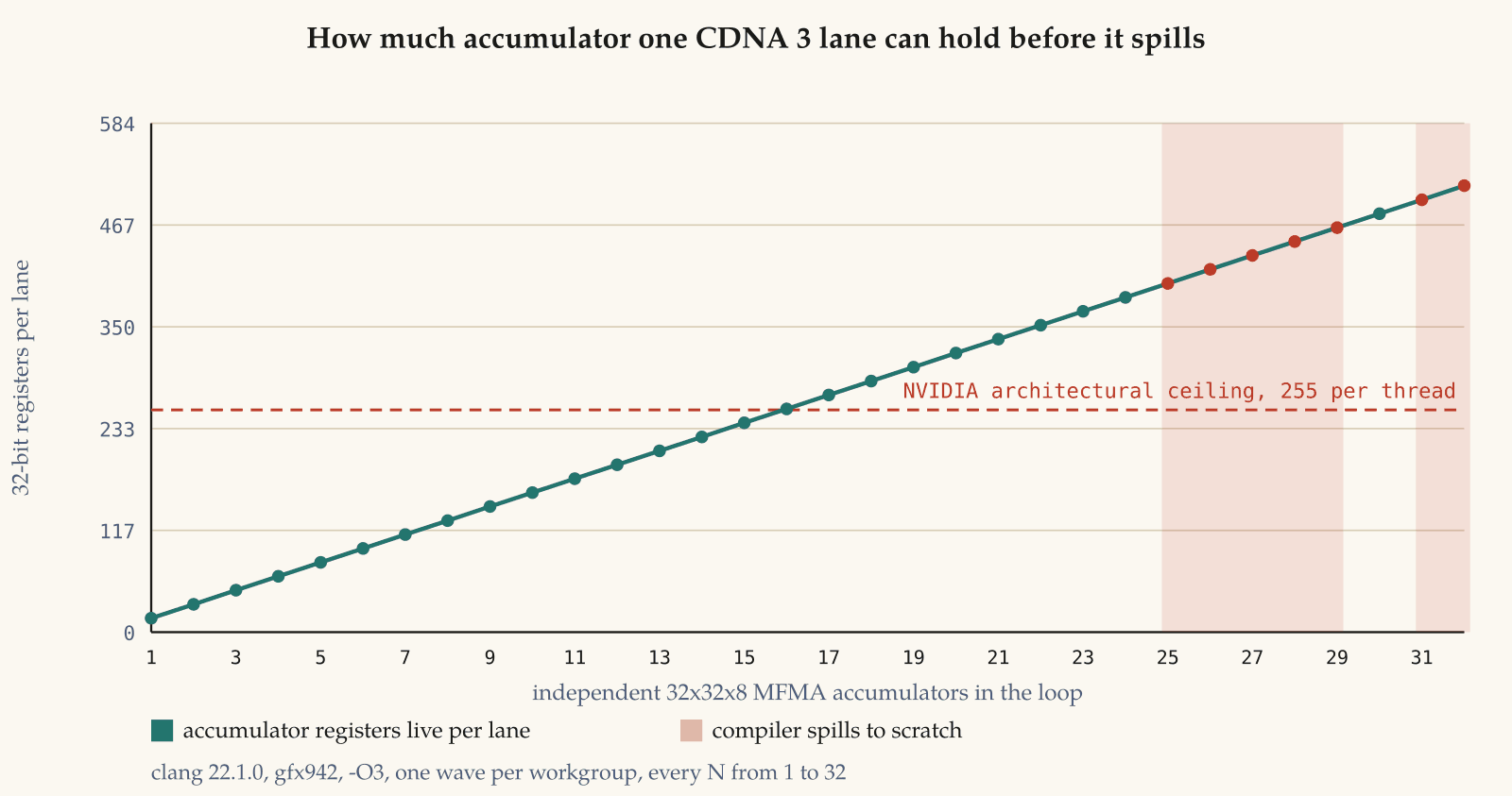
The shape of that curve is the answer. Up to eight accumulators, 128 registers of live state, everything sits in ordinary vector registers. At sixteen the accumulator alone needs 256 registers and the allocator crosses a line: 288 registers total of which 32 are AGPRs, with ACCUM_OFFSET set to 256 in the kernel descriptor.
At twenty four, 384 registers of live accumulator, it has allocated the entire 512 entry file with 256 of those entries as AGPRs and still spills nothing. Twenty five is where scratch traffic starts.
The tail is not monotone, and it is worth saying so because I got it wrong the first time I looked. Twenty five through twenty nine spill; thirty does not, allocating 500 registers and reaching 480 of live accumulator; thirty one spills 512 bytes.
The allocator is finding a different schedule at that one point rather than the file getting bigger. The defensible ceiling is twenty four accumulators.
So the answer is that on CDNA the same problem does not arise. A CDNA lane has 512 architectural registers, not 255. The file is one physical structure that the kernel descriptor partitions at a byte offset into a general half and an accumulator half, and matrix instructions can name the accumulator half directly.
There is no new address space, no allocator, no separate instruction family for moving results in and out, no class of guardrail trap. The thing NVIDIA had to invent an address space for, AMD had already solved in 2020 by making the register file twice as deep and teaching the descriptor where to cut it.
That is not a rhetorical point, and it generalises into a number worth having. If you divide the on-chip state a unit owns by the matrix throughput that unit can sustain per clock, you get bytes of working set per unit of arithmetic, which is the ratio that decides whether the accumulator fits.
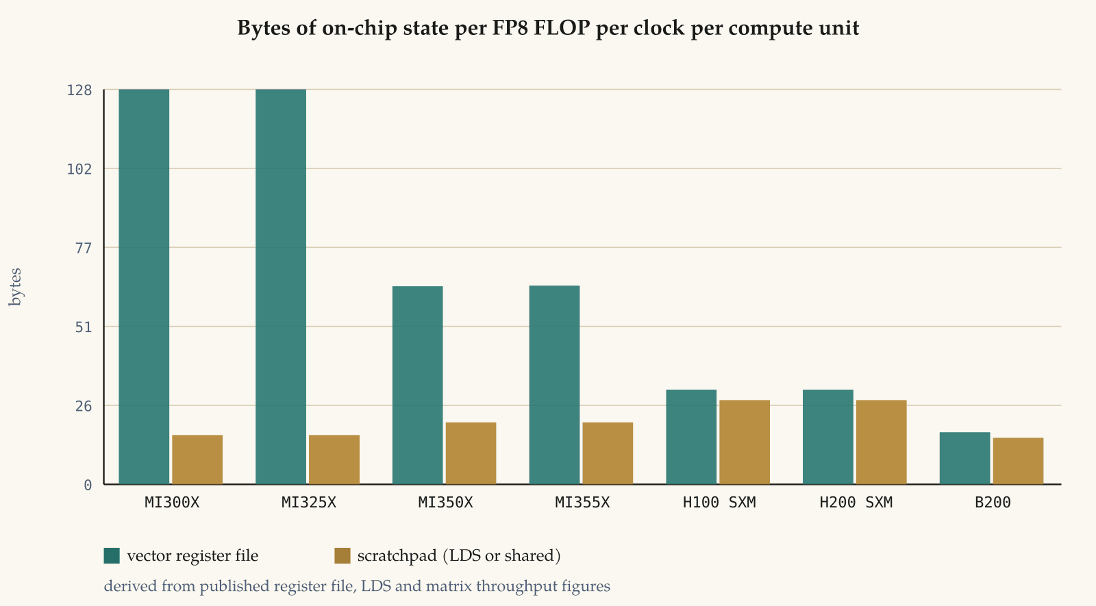
An MI300X compute unit carries roughly 144 bytes of register file and scratchpad for every FP8 FLOP per clock it can issue. An H100 SM carries 58. A B200 SM carries 32.
NVIDIA has cut that ratio by roughly a factor of four and a half across two generations, because matrix throughput per SM doubled twice while the register file did not move at all and shared memory did not move at all.
AMD’s CDNA 4 cut its ratio too, from 144 to 85, by doubling matrix throughput per CU while holding the register file at 512 and raising the LDS from 64 KB to 160 KB. It is still two and a half times richer than Blackwell.
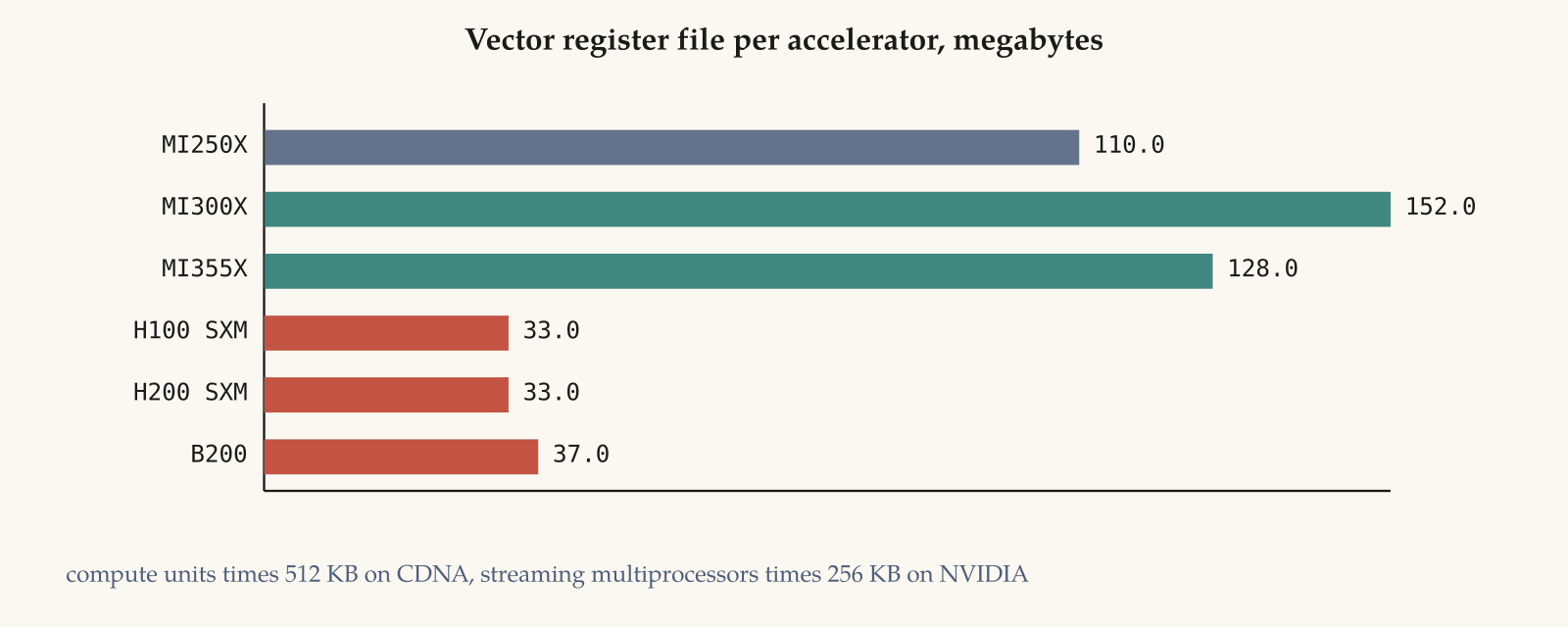
Read the two histories side by side and the divergence is legible. NVIDIA has been spending down on-chip state per FLOP as fast as it can and buying it back with mechanisms: asynchronous copy, then the tensor memory accelerator, then a dedicated accumulator memory.
Each is a way of not paying for registers. AMD kept paying, which is why its kernels can be written in a flatter style and why an MI300X carries 152 megabytes of vector register file against an H100’s 33.
Neither choice is obviously right. NVIDIA’s buys throughput per millimetre and pays in programming model complexity, which it absorbs by shipping libraries that hide the complexity, a business it is good at.
AMD’s buys a simpler programming model and pays in area, which is a reasonable trade if your pitch is that the customer can write the kernel themselves.
Matrix cores, concretely
A representative MFMA, v_mfma_f32_32x32x8_f16, computes a 32 by 32 by 8 product with FP16 inputs and an FP32 accumulator, executed collectively by one wavefront, with operands and result distributed across lanes in a fixed layout the programmer has to know.
The A operand is four halves per lane and the accumulator sixteen floats per lane; 64 lanes times sixteen floats is the 1,024 values of the 32 by 32 tile.
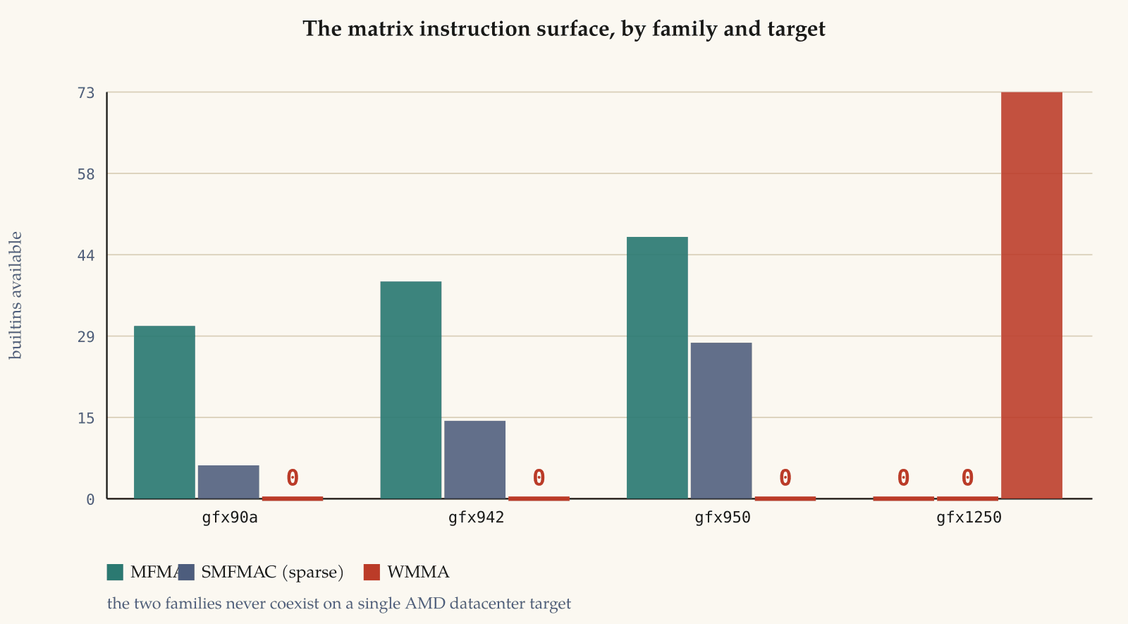
The family is large and grew fast. In LLVM 22, gfx90a exposes 31 MFMA builtins, gfx942 39, gfx950 47, with the sparse SMFMAC family going 6, 14, 28 across the same three and conversions going 7, 15, 66.
CDNA 4’s contribution is almost entirely data types: block-scaled FP8, FP6 and FP4 in the OCP microscaling format with a shared 8 bit exponent per 32 elements, plus the scaled instructions to consume them, of which v_mfma_scale_f32_16x16x128_f8f6f4 is the one you meet in a real MXFP4 GEMM.
Two practical facts about using these that are worth more than a page of theory.
The first is that the smaller tile usually wins. AMD’s own guidance says the 16x16 form outperforms the 32x32 form on MI300X for GEMM, including at large sizes, and gives the reason as power efficiency rather than issue rate.
This is the sort of thing that is invisible from a spec sheet and decisive in practice, and it is why Triton exposes matrix_instr_nonkdim as a tuning knob at all.
The second is that on CDNA 4 you should match BLOCK_K to the instruction’s K dimension and aim for one or two matrix instructions per K step. FP16 wants v_mfma_f32_16x16x32 with BLOCK_K 64.
FP8 wants v_mfma_f32_16x16x128 with BLOCK_K 128. MXFP4 wants the scaled instruction with BLOCK_K 256. Get that wrong and you pay pipelining overhead on every step of the loop.
A third fact says more than either about where performance comes from. AMD’s tuning guide reports that in its own reference Gluon GEMM for gfx950, switching the operand path from staging through registers to buffer_load_to_lds, a direct L1 to LDS asynchronous copy, moved the kernel from 697 to 1113 TFLOPS.
Sixty percent from one instruction selection decision, and the stated mechanism is that it saves roughly 100 VGPRs per wave and deletes a register movement phase from the loop.
The same document reports that remapping workgroup ids so consecutive tiles land on the same XCD cut L2 misses from circa five million to 3.1 million and added another 67 TFLOPS.
Hold that against the register file. The async copy is worth sixty percent because it returns a hundred registers to the accumulator, and registers are what this architecture spends its area on. The architecture and the kernel technique are one fact seen from two sides.
Eight dies pretending to be one GPU
An MI300X is not a chip. It is eight compute dies on four I/O dies with eight HBM stacks, and an MI350X is eight compute dies on two I/O dies with a faster link between them. This has consequences that leak through every abstraction above it.
Each XCD has 40 physical compute units of which 38 are enabled on MI300X, its own 4 MB L2, and its own hardware scheduler. The 256 MB Infinity Cache sits on the I/O dies, in front of memory, shared.
So the cache hierarchy is not a tree with a single root: it is eight private L2s and one shared last level, and two workgroups that share data are cheap if they land on the same XCD and expensive if they do not. There is no hardware mechanism that makes this decision for you.
The mechanism is that workgroups are handed to XCDs round robin, and therefore if you want two tiles co-resident you remap your program id arithmetic so that they are congruent modulo eight.
AMD’s guidance to use workgroup mapping values that are multiples of the XCD count is exactly this, and you can see it in the shipped kernel names: WGMXCC8 appears in the GEMM library’s solution names because the number eight is baked into the tuning.
Two more things about this die that would be folklore elsewhere. Clock speed varies between XCDs on the same package by three to ten percent, XCD0 typically fastest and XCD7 slowest on MI300X, so an efficiency number computed against nominal clock is systematically optimistic and AMD tells you to compute against the slowest XCD.
And a GEMM whose leading dimension is a multiple of 512 bytes hits channel hotspotting, with the recommended fix being to pad: lda = ldb = K + 128 when K is a multiple of 256. Every memory system has stride pathologies. It is unusual to be told about them.
Partitioning is the other side of the chiplet story. An MI300X can be presented to software as one device with eight XCDs and 192 GB, or two, or four, or eight devices with one XCD and 24 GB each, in modes named SPX, DPX, QPX and CPX, crossed with memory interleaving modes NPS1 through NPS4.
AMD recommends QPX with NPS4 on MI300X and DPX with NPS2 on MI350X. For a serving fleet this is a real knob: a model that fits in 24 GB gets eight independent devices per module with no cross-device traffic at all, which is a different machine from the one on the spec sheet.
The numerics fork, which cost more than it should have
Now the part of the story that is a genuine unforced error, and the best available evidence that a numerics contract is a moat in its own right.
FP8 has two dialects. The OCP standard E4M3 has an exponent bias of 7, supports both signed zeros, and has NaN encodings. The variant AMD implemented on CDNA 3, called E4M3FNUZ, has an exponent bias of 8, a single zero, and one NaN. The bit layout is the same.
The value the bits mean is not: read an FNUZ byte as if it were OCP and you are off by a factor of two.
CDNA 4 switched to the OCP variant. So the MI300X and MI325X speak one FP8 and the MI350X and MI355X speak another, and a checkpoint quantised on NVIDIA hardware speaks the second.
In practice this means every FP8 path in every framework has to be conditioned on the architecture at runtime, and the condition is a function call that asks the driver what chip it is talking to.
It went about as well as you would expect. In June 2026 a vLLM issue documented that the sparse attention wrappers for a MiniMax model classified only float8_e4m3fn and float8_e5m2 as FP8, omitting float8_e4m3fnuz, so on gfx942 the KV cache bytes were reinterpreted in the wrong dialect before the attention kernels consumed them, with an accuracy loss on a 1,319 sample GSM8K run that the fix recovered.
In the same period an AITER issue reported that building for two architectures at once, GPU_ARCHS=gfx942;gfx950, made the dtype helper return the OCP type on an MI300X, because it resolved the architecture from the build configuration rather than the device.
Fergus Finn, bringing up DeepSeek V4-Flash on a single MI300X, wrote that many of vLLM’s FP8 paths know E4M3 from E5M2 but not FNUZ from OCP, and observed that MI300X is the only major accelerator where the distinction matters in practice.
That last “clause” is about the whole cost. A format that only one vendor’s one generation uses gets tested by exactly the people who have that hardware, which is a small fraction of the people who write the code.
Being different is expensive in proportion to how few of you there are, and it is expensive in the layer where it is hardest to notice, because the failure mode is not a crash, it is a slightly worse answer.
Two more numerics changes in CDNA 4 deserve a line. TF32 moved from hardware to software emulation via BF16, which sounds like a regression and is not, because BF16 matrix throughput on CDNA 4 is 4,096 FLOPs per clock per CU against CDNA 3’s TF32 rate of 1,024, so the emulated path is faster than the hardware path it replaced.
And FP64 matrix throughput halved, from 256 to 128 FLOPs per clock per CU, which is a deliberate reallocation of area away from HPC toward AI and is the reason AMD now ships a separate HPC part.
Counting the kernel layer
Here is the measurement I most wanted to make, and the one that is only possible because the stack is open.
hipBLASLt’s GEMM kernels are generated by TensileLite, an assembly generator, and the decision about which generated kernel to use for a given problem shape lives in YAML files in the repository. I cloned the logic directory and counted it.
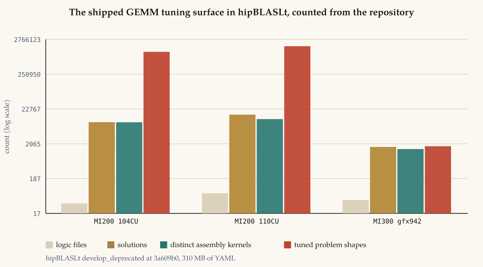
145 logic files. 26,248 solutions. 16,177 distinct assembly kernel names. 2,905,048 entries mapping a problem shape to a solution index. 310 megabytes of YAML, of which 297 MB is the tuning tables.
Two details in that census are worth more than the headline. The first is that the MI200 tuning is split into directories named 104CU and 110CU. The same architecture, tuned separately by how many compute units were left enabled after harvest.
Which bin of the die you bought changes which kernel is fastest for your matrix, and the library ships both tables. The second is that the older architecture has vastly more tuned shapes than the newer one: MI200 carries 2.9 million exact entries across two CU counts, while the gfx942 tree in this snapshot carries 1,746, because MI300’s dispatch leans much harder on heuristics and grid-based interpolation than on exhaustive tables.
Then I did something with the kernel names, because Tensile’s names are self-documenting. A real one, unedited:
Cijk_Ailk_Bjlk_BBS_BH_Bias_HAS_SAV_UserArgs_MT256x224x32_MI16x16x1_SN
_GRVWA8_GRVWB4_GSU2_LBSPPA2048_LBSPPB1792_LPA0_LPB32_MIWT4_14_NTC0
_NTD0_NLCA1_NLCB7_SU8_SUM0_SUS256_SVW4_VWA4_VWB2_WSGRA0_WSGRB2
_WG64_4_1_WGM304_WGMXCC8_WGMXCCG0
MT256x224x32 is the macro tile. MI16x16x1 is the matrix instruction. GRVWA8 is the global read vector width for A. GSU2 is global split-U. WGM304 is a workgroup mapping value that happens to be the compute unit count of the part.
Parse all 1,439 distinct gfx942 names and you recover the search space directly:
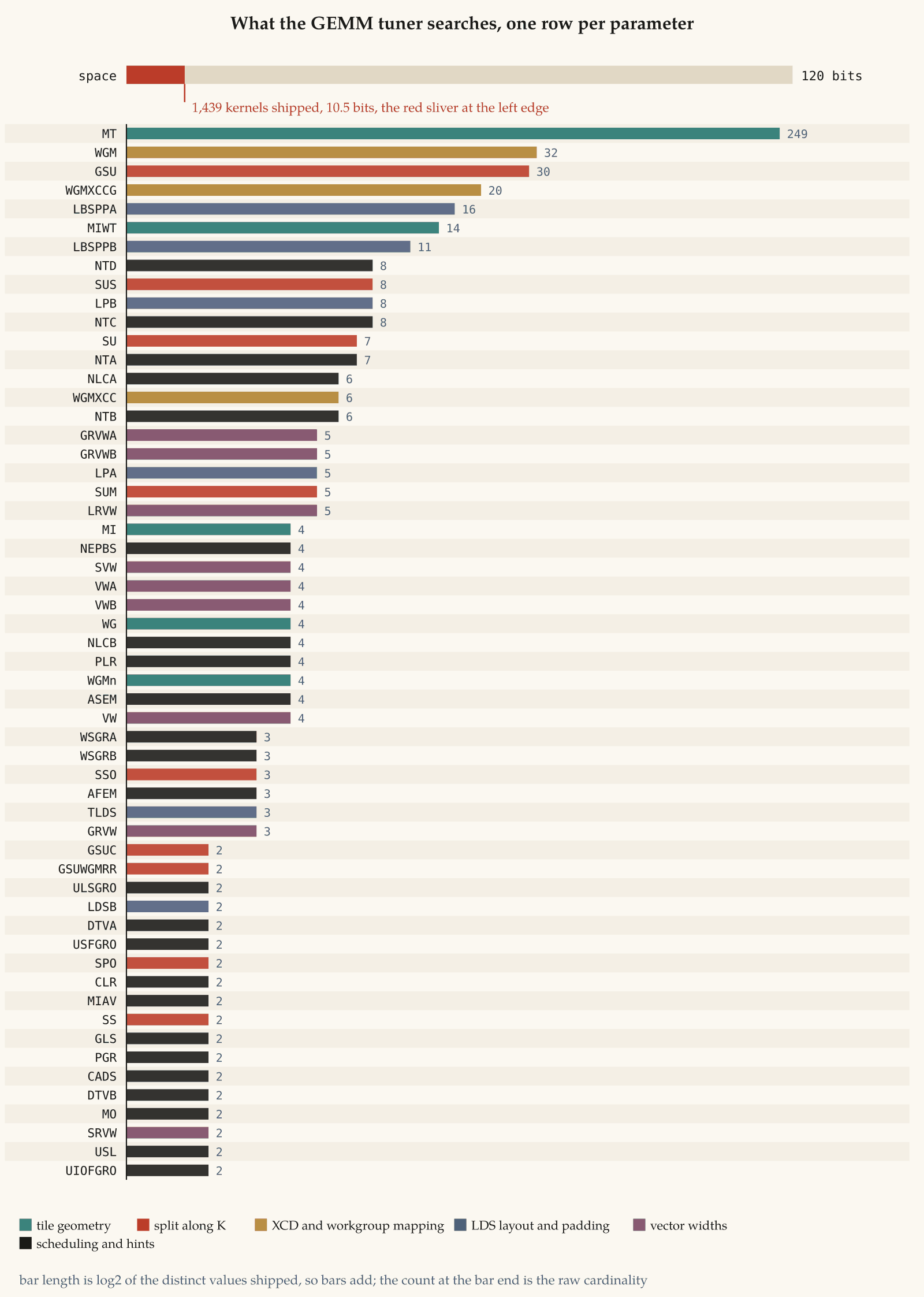
Fifty six parameters take more than one value across the shipped set. Because cardinalities multiply, the natural unit is bits: a parameter with sixteen observed values contributes four. They sum to 120 bits, which is 1.3 times ten to the thirty sixth. The 1,439 kernels actually shipped are ten and a half bits of that.
Where the bits sit is as interesting as how many there are. Scheduling and non-temporal hints carry 39 of them across 24 parameters, more than tile geometry and K splitting combined.
The macro tile alone is eight bits, and the three XCD mapping parameters are twelve, which is a lot of search space spent on the fact that the chip is eight dies.
That is what the kernel layer is. Not a secret, not a compiler trick, not a set of instructions nobody knows about. It is a search over a space with about thirty six log-decades of volume, resolved by measurement on real silicon, and then frozen as a lookup table. The library is the record of the search.
Which is why I have been arguing for a while that the correct model of this moat is a labour market rather than a technology, and this measurement is the strongest version of that argument I have been able to construct. Anybody can read the ISA. Anybody can write the assembly.
What is truly expensive is running the 2.9 million benchmarks on hardware you have to own, and doing it again for every new part, and again for every harvest bin of every new part.
Four compilers, one backend
The compiler story is simpler than people expect, because there is one backend and it is upstream.
Every path into a CDNA GPU ends at the LLVM AMDGPU target. HIP is clang. OpenMP offload is clang. Triton’s AMD backend emits LLVM IR into the same code generator. Composable Kernel is C++ templates compiled by clang. Even the assembly generators emit text the same assembler consumes.
There is no split where a public virtual ISA is compiled by a private program into the real one: the .s file clang produces is the instruction stream, and llvm-mc assembles it back.
So the surface area of AMD’s compiler is measurable, and it is growing fast. The AMDGPU builtin list went from 443 entries in LLVM 20.1.2 to 788 in 22.1.0, up 78 percent with nothing removed. Available per target: 244 on gfx90a, 274 on gfx942, 362 on gfx950, 477 on gfx1250.
Triton is the most important of the four paths, because it is the one the frameworks generate into. The AMD backend is real and it is used in production: TorchInductor generates Triton, vLLM ships Triton attention kernels for ROCm, and AMD’s own guidance for tuning them is specific in a way that tells you what the compiler is not doing for you.
Set num_stages to 2 for a single GEMM and 1 for two fused GEMMs, because the pipeliner’s cost model does not know the difference.
Use waves_per_eu to push the register allocator down to the next occupancy step, because the allocator optimises for spills rather than occupancy. Use matrix_instr_nonkdim to pick the matrix instruction, because the heuristic picks the larger one and the smaller one is usually faster.
Each knob is a place where the compiler has a policy and the policy is wrong often enough to warrant a flag. That is the state of the art everywhere, not an AMD failing, but the flags read as a map of the gap.
Gluon is the interesting recent addition. It ships alongside Triton, compiles through the same IR, and exposes what Triton hides: explicit layouts, explicit asynchronous copies and barriers, explicit LDS placement.
AMD’s documentation is unusually frank about when to reach for it, namely when the profiler shows you bottlenecked on layout conversions, matrix instruction selection or pipelining depth, which is to say on the three decisions Triton makes for you. The 697 to 1113 TFLOPS figures come from that tutorial.
A sixty percent gap between the natural expression and the tuned one, in a kernel the vendor wrote to demonstrate tuning, is an honest measure of how much the language is doing.
Composable Kernel is the older answer: a C++ template library where a kernel is assembled from tile descriptors and instances are enumerated at build time.
TorchInductor can use it for GEMM if you add CK to the autotune backends, and it is one of AITER’s. Its weakness is the one every heavy template library has, and the fact that AITER ships Opus, a single-header alternative advertised as up to 61 times faster to build, is a fairly direct comment on it.
What actually runs when you serve a model
AITER is the piece that changed the trajectory, and “AMD’s cuDNN” undersells it.
AITER is a dispatcher with five backends: Composable Kernel, hand-written assembly, Triton, a DSL called FlyDSL, and hipBLAS. For a given operator and shape it picks one, driven by CSV tables of tuned configurations merged at runtime with model-specific tables shipped alongside.
In vLLM it is one environment variable, VLLM_ROCM_USE_AITER=1, and it replaces GEMM, RMSNorm, mixture-of-experts and attention kernels underneath the engine without the model code changing.
Attention shows the design working. For multi-head latent attention, vLLM on ROCm offers a Triton backend and two AITER backends that differ only in the prefill path: both use the same hand-written assembly decode kernel, mla_decode_fwd, and vLLM’s own write-up attributes most of the 1.2 to 1.6 times speedup to that one kernel, because decode is memory bound and time per output token is decode-heavy.
What that bought is visible from outside AMD. SemiAnalysis’s InferenceX v2, published in February 2026, measured MI300X SGLang throughput roughly doubling between December 2025 and January 2026. Same silicon, same model, one month, two times the tokens. That measurement settles the question of whether the hardware was the constraint.
It also says something uncomfortable about every AMD benchmark published before it. A number measured on ROCm in November 2025 was not measuring the machine; it was measuring the kernel library at a moment in a period of rapid change. Hold that when reading anybody’s AMD versus NVIDIA comparison, including the ones I cite approvingly.
The version story compounds this. ROCm currently ships in two parallel streams, with 7.0 through 7.8 reserved for production and 7.9 and later designated as a technology preview with a different build system, so the highest version number is not the production one.
As of this writing production is 7.2.x and preview is 7.14. Meanwhile hipBLASLt’s default branch on GitHub is named develop_deprecated and its head commit is from June 2025. None of these are disasters, but collectively they are the texture of a stack that is being rebuilt while in flight, and they are a real cost to anybody trying to pin a reproducible configuration.
The arithmetic, which is where AMD’s case is strongest
Strip away the software argument for a moment and ask what the hardware is for.
The batch at which a dense GEMM stops being memory bound and starts being compute bound is a property of the part, not of the model. Call it B*, and it is peak throughput times bytes per element divided by twice the memory bandwidth.
The reason it is worth computing is that it is invariant to precision: peak throughput scales as the inverse of element width, so the product is a constant for a given generation, and quantising a model moves the ceiling without moving the corner.
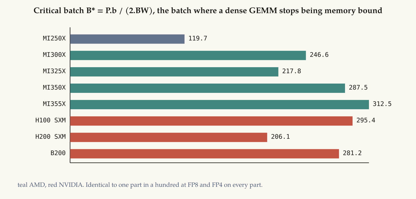
MI300X sits at 247. H100 sits at 295. MI350X at 288, MI355X at 313, B200 at 281. Every one is identical across FP16, FP8 and FP4 to within one percent, a third independent confirmation of the invariance on silicon I had not previously tested it on.
So MI300X reaches the compute-bound regime at a batch about sixteen percent smaller than H100 does, a real advantage for interactive serving, and by the current generation the two vendors have converged to within ten percent. Whatever quantisation is buying, it is not an escape from the memory wall.
Then run the same arithmetic on what is shipping now. AMD’s product page gives MI455X 20 PFLOPS of FP8, 40 of FP4 and up to 23.3 TB/s of HBM4. That puts B* at 429, up thirty seven percent in one generation. NVIDIA’s published Rubin figures move in the same direction.
The corner that barely moved for two generations is now moving quickly, and it is moving the wrong way for the argument AMD has been making, because the memory-bound regime where a less mature kernel layer costs you little is the regime that is shrinking.
I would not over-read a single generation. But if I had to name the thing most likely to invalidate the AMD inference case over the next two years, it would not be software. It would be this number.
The place the arithmetic is not close is capacity.
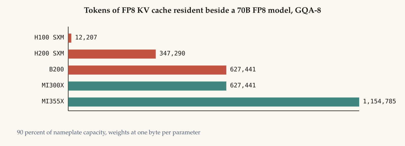
Take a 70 billion parameter dense model with grouped query attention at eight key-value heads, weights and KV cache both at one byte per element, and give the runtime ninety percent of nameplate memory.
H100 has two gigabytes left for KV after the weights, which is about twelve thousand tokens, which is one and a half concurrent requests at eight thousand tokens of context.
MI300X has 103 gigabytes left, which is 627,000 tokens, which is 76 concurrent requests.
Whereas, an MI355X has 189 gigabytes left, 1.15 million tokens, 141 requests.
We see there’s a fifty times difference between an H100 and an MI300X in the quantity that determines how many users one accelerator can serve at once, and it required no software from anybody.
H200 closes most of it and B200 closes the rest, which is why the AMD capacity advantage was a 2024 and 2025 story more than a 2026 one, but it is also why AMD got the foothold it got: for a period, the only way to serve certain models without sharding was on AMD.
The current generation’s claim is narrower and more credible for being narrower. AMD says a Helios rack delivers up to 30 percent more tokens per dollar than the leading competitive solution, based on its own labs, with the MI455X carrying 432 GB of HBM4 against Rubin’s 288 and the rack pooling 31 TB.
Thats a capacity argument again, dressed as an economics argument, and it will be right or wrong depending on whether the kernels exist.
What a port actually costs
The official story about moving code from CUDA to ROCm is HIP plus hipify: run a translator, get a source tree that compiles for both, done. A figure of roughly 92 percent coverage of CUDA device APIs circulates in reseller and channel material around the MI355X launch.
I couldn’t trace it to a primary AMD statement, so treat it as folklore with a plausible magnitude rather than as a specification.
Whatever the true figure, it is the least interesting number in the discussion, because the remainder is not randomly distributed. It concentrates in exactly the places where performance lives.
Consider what does not port. Inline PTX, because there is no PTX. Warp level primitives with hardcoded masks, because the mask is 64 bits wide.
Anything using the tensor memory accelerator, wgmma or tcgen05, because those mechanisms do not exist and the matrix instructions have different shapes and register layouts. CUTLASS, where a great deal of the industry’s kernel expertise is encoded, is structurally NVIDIA-specific from the CuTe layout algebra down.
Anything assuming 32 lanes per warp for a reduction is subtly wrong rather than broken, which is worse. And numerics do not port, as the FNUZ story demonstrated at length.
The honest description of a port, then: the model runs almost immediately and the kernels that make it fast do not exist. That matches every bring-up worklog I have read.
A model comes up in a day, then weeks go into finding which operator fell back to a slow path, which is what you would predict from a stack whose framework layer is portable and whose kernel layer is a per-architecture lookup table.
One naming artefact tells the whole story. PyTorch on ROCm still calls the device cuda: torch.cuda.is_available() returns true, tensor.cuda() works.
The build hipifies PyTorch’s sources and keeps the Python-facing names, because changing them would break every model script in existence. The API surface is compatible and the thing underneath is not the same machine.
Profiling, and the churn
The profiling story is the part of ROCm that has changed most in the last two years and it is worth knowing where it landed.
The current tools are rocprofv3 for counters and traces, ROCm Compute Profiler (formerly Omniperf) for guided kernel analysis, and ROCm Systems Profiler (previously known as Omnitrace) for whole-application timelines.
The generation before, rocprof, rocprofv2, ROCProfiler and ROCTracer, is deprecated with end of support announced for the second quarter of 2026, and as of the 7.2.1 notes PyTorch on ROCm still depended on ROCTracer, with a known issue tracking the migration.
That is a fair sample of the ROCm experience: the new tools are good, the migration is real, the documentation is honest about what has not moved, and something you depend on is probably still on the old path.
The counter model is conventional. Per-shader-engine and per-cache counters, collected in multiple passes with the application re-run each time, so anything nondeterministic is measured across different executions.
For a matrix kernel the ones that matter are MFMA issue counts, L2 and Infinity Cache hit rates, and memory controller requests, and the derived metrics sit close enough to Nsight Compute’s sections that the mental model transfers.
One capability has no clean counterpart: advanced thread trace, which captures per-instruction issue timing inside a wave. Combined with being able to read and rewrite the instruction stream using standard tools, it closes the loop of look at the schedule, change the schedule, measure the schedule, which is hard to close on the other side.
Whether anyone outside AMD runs that loop at scale is a separate question, and I suspect the answer is a few dozen people.
What the numbers say about the machine, not the marketing
One last piece of arithmetic before the fork, because it reframes the generational comparison in a way the press releases do not.
Peak throughput figures conflate three things: how many units there are, how fast they run, and how much each unit does per clock. Divide it out and you get the architectural quantity.
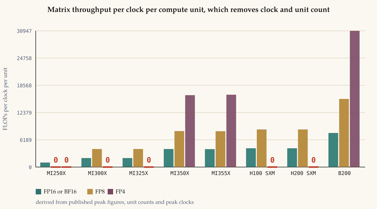
An MI300X compute unit does 2,048 FP16 and 4,096 FP8 FLOPs per clock. An H100 SM does about 4,271 and 8,543. So per unit per clock, a CDNA 3 compute unit is half an H100 SM, and AMD reaches parity on the total by fielding 304 units against 132 and by accepting more area and more power.
CDNA 4 doubles the per-unit rate to about 8,138 FP8, which lands on top of Hopper, and adds FP4 at 16,439. Blackwell doubles again to 15,473 FP8 and 30,947 FP4.
That is the real generational story and it is more interesting than the PFLOPS. AMD spent CDNA 4 catching the previous NVIDIA generation on matrix density per unit while cutting unit count from 304 to 256, and paid for it with process, going from N5 to N3P. NVIDIA spent the same interval doubling again.
On matrix density per compute unit per clock, the gap between the two current parts is close to a factor of two, and the gap on the whole part is much smaller because of unit counts and clocks.
Which is why the AMD case has always been strongest where matrix density is not the binding constraint, which is decode. Decode is memory bound below B, which is 313 on MI355X and 281 on B200, and the memory bandwidth is the same 8 TB/s on both.
In that regime a compute unit that does half the matrix work per clock is not costing you anything, and 288 GB against 192 is costing the other side quite a lot.
The AMD inference argument, stripped of everything else, is that a large fraction of served tokens are generated in a regime where the thing AMD is worse at does not bind and the thing AMD is better at does.
That argument was correct in 2024, it survived the H200, and the MI455X version of it, 432 GB against 288, is the same argument again.
Whether it holds depends on kernels that, as of this writing, are being written for an instruction set that did not exist eighteen months ago.
Why the case is inference and not training
There is a persistent asymmetry in AMD’s results that I have seen stated as a puzzle and that I think has a clean explanation. AMD is competitive on inference, sometimes better than competitive, but is not even close on training.
The usual explanation is that training software is harder, which is true and unhelpful. The specific version is more useful, and it falls out of the structure described so far.
Start with what a kernel layer costs to build. A serving engine’s hot path is a small set of shapes: attention in its prefill, extend and decode forms, the projections, the mixture-of-experts grouped GEMM, the normalisations, the sampling tail. Perhaps twenty operators, each with a handful of shape families fixed once you pick the model.
That is a finite, enumerable target, and it is why AITER can exist as a dispatcher with per-model CSV tables. You can hand-write assembly for a decode kernel because there is one decode kernel and it stays hot for the life of the model.
Training is not that. Backward passes roughly triple the operator count and introduce transposed shapes that hit different tuning entries. Optimiser state is bandwidth-bound elementwise work over parameter-sized tensors.
Gradient collectives at every step put the interconnect on the critical path rather than at the margin. It runs for weeks, so numerical drift invisible in a benchmark becomes a divergence at step 40,000, and it runs across thousands of accelerators where the binding constraint is not any kernel but the probability that all of them stay up.
None of that is helped by a deep tuning table, because there is no hot shape you can pay somebody to tune once.
Then the collective asymmetry. On a fully connected eight-way node, all-reduce at full width is efficient, which is what AMD’s use-eight-or-one guidance reflects. Above the node you are on the scale-out fabric, and until Helios there was no rack-scale scale-up domain at all. A tensor-parallel group that fits in a node is fine.
One that does not, or an expert-parallel all-to-all spanning racks, is the problem NVIDIA spent NVL72 on two years earlier.
Now apply the same reasoning to inference and the picture inverts. Decode is memory bound below B*, which we computed at 247 on MI300X and 313 on MI355X. Below that batch, matrix throughput per compute unit is not the constraint, which neutralises AMD’s largest architectural deficit.
Capacity is the constraint, and AMD has more of it, by 50 percent against B200 on the current part and by 50 percent again on the next one. Prefill is compute bound and AMD is worse there, but prefill is amortised across the output tokens of a request, and for the long-output workloads that dominate agentic and reasoning traffic, that amortisation is generous.
So the asymmetry is not primarily a software story. It is that inference has a small hot kernel set, tolerates a per-model tuning table, lives in a regime where AMD’s weakness does not bind, and puts a premium on the quantity AMD sells the most of.
What the money looks like
Let me be careful here, because I am about to do arithmetic on numbers I did not measure, and the conclusions are only as good as the inputs.
The best third-party source is SemiAnalysis’s InferenceX, which publishes a continuously updated benchmark rather than a single number, and the trajectory of that benchmark is more instructive than any point on it.
On 20 May 2026 InferenceX measured MI355X on SGLang FP8 as up to about 40 percent cheaper per million tokens than B200 on GLM-5 at 8K input and 1K output, with the peak gap at 18 tokens per second per user, 22 cents per million against 30. B200 took the lead back above roughly 90 tokens per second per user.
Two months later the same benchmark’s overview, running its July TCO model, listed MI355X at 35.5 cents per million on the 8K/1K FP4 path against B200 at 30.4, which is 17 percent the other way.
On the long-context multi-turn agentic scenario the gap in the published table is close to an order of magnitude in NVIDIA’s favour, and I would want to read that methodology carefully before leaning on the magnitude.
Nothing about the hardware changed in those two months. What changed is that B200’s NVFP4 path shipped for that model, and that AMD still has no disaggregation or wide expert parallel recipe for it while NVIDIA’s rack-scale version demonstrated roughly three times the throughput per GPU from wide expert parallelism alone.
That cuts against the argument I would otherwise have been tempted to make. A cost-per-token comparison between these two vendors is not a fact about the machines. It is a snapshot of which recipe landed most recently, and it has flipped sign twice inside one quarter.
AMD’s Helios claim, up to 30 percent more tokens per dollar than the leading competitive solution, is a very different object again: a projection about a rack that began shipping at the end of the third quarter, against a competitor rack, from AMD’s own labs. Weight it accordingly.
The mechanism survives the specific numbers going stale, so state it in the abstract. Cost per token for a memory-bound decode is the accelerator hour rate divided by tokens per hour, and tokens per hour is roughly bandwidth over bytes touched per token, times the concurrency you can hold.
AMD’s argument is that the rate is lower because AMD sells at a discount and the concurrency is higher because AMD ships more memory. Neither depends on kernels being good, only on their not being bad enough to cost you the bandwidth.
That last clause is the whole game, and it is measurable. If a kernel achieves 80 percent of peak HBM bandwidth on decode, and the competitor’s achieves 90, then the entire kernel gap is 11 percent, and it is bounded above by the ratio of achieved bandwidths regardless of how much cleverness is in the other stack.
This is a much tighter bound than the equivalent for a compute-bound kernel, where the gap between a naive and a tuned implementation can be five times or more.
It is the analytical reason a memory-bound regime is forgiving of a less mature kernel layer, and it is the reason AITER could double throughput in a month and then not double it again.
The corollary is uncomfortable for the AMD case in a different direction. Once a workload moves into the compute-bound regime, above B*, the forgiving bound disappears and the kernel gap opens back up to whatever the tuning tables say it is.
Batch sizes are going up, prefill-heavy agentic traffic is going up, and speculative decoding exists specifically to manufacture arithmetic intensity. Every one of those trends moves served traffic toward the regime where AMD’s kernel maturity matters more, not less.
The three numbers I would want if I were buying
If somebody put a purchase decision in front of me, I would want three measurements and would not care much about anything else.
The first is achieved HBM bandwidth on decode for the specific model, as a fraction of nameplate, on both candidate machines, measured on the same day with the same serving engine version. That single ratio bounds the kernel gap in the regime where most tokens are produced, and it is cheap to measure.
The second is the fraction of end-to-end wall clock spent in operators that fall back to an untuned path. On AMD this is directly observable: run with the tuning tables and without, and the difference is the size of the table’s contribution. If the answer is large, you are buying a dependency on the vendor’s tuning campaign continuing.
The third is the date on every number in the deck, from either vendor. A third party measured a two times throughput change in a month and a sign flip in cost per token inside a quarter. Any figure older than that is not evidence about the machine you would receive.
And if the machine in question is an MI455X, I would add a fourth, which is what fraction of the operator set has a gfx1250 kernel at all, as opposed to a Triton fallback. That number is knowable, it changes weekly, and as of this writing I have no way to measure it from outside.
The fork
Which brings us to the measurement I opened with.
I ran the entire clang builtin table against the target feature sets of five AMD datacenter targets, which is exactly the computation clang performs when it decides whether to accept a builtin, and then verified a sample of the results by compiling.
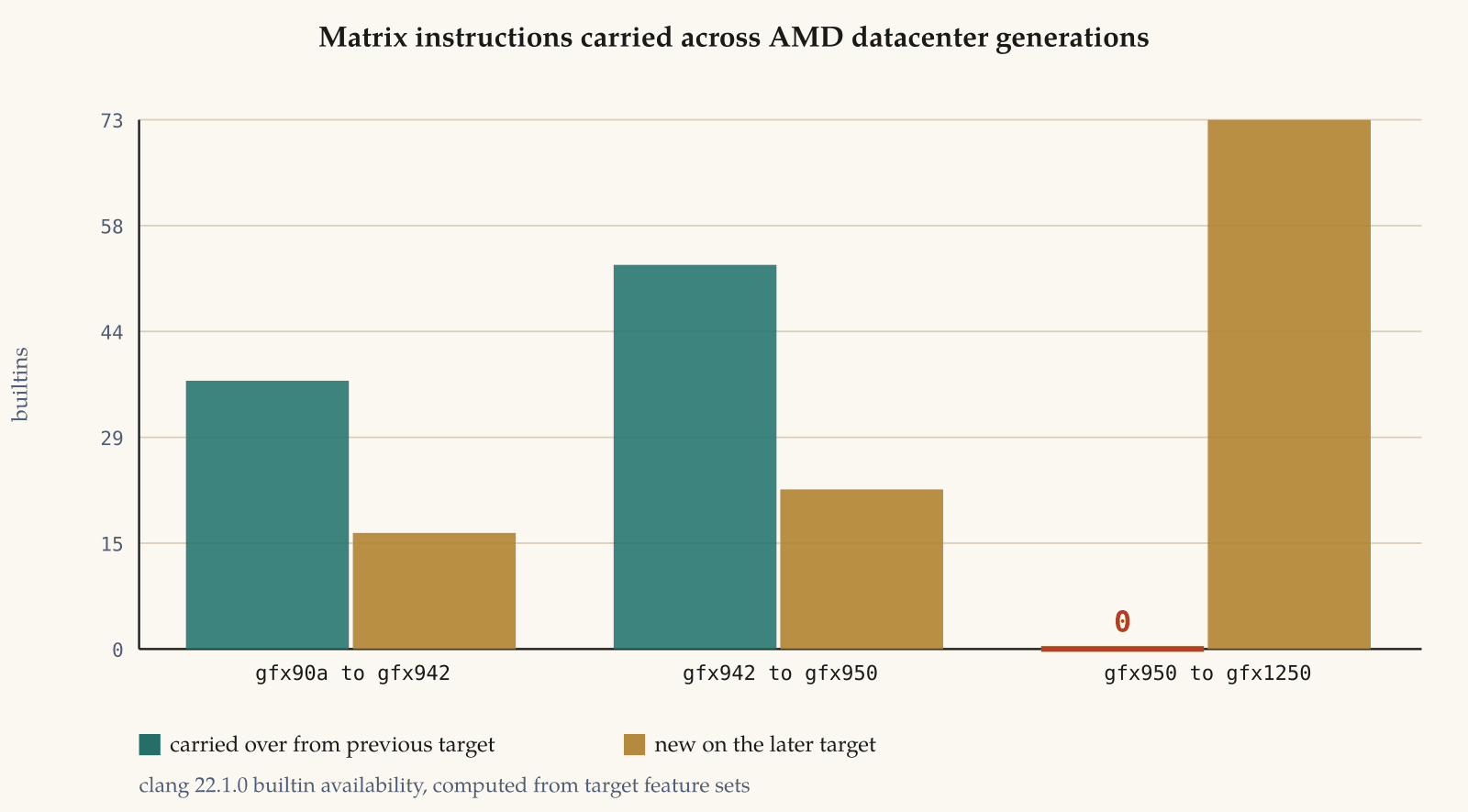
From gfx90a to gfx942, 37 of 37 matrix builtins carry over, and 16 are added. From gfx942 to gfx950, 53 of 53 carry over, and 22 are added. From gfx950 to gfx1250, 0 of 75 carry over, and 73 appear that did not exist before.
The empirical check is straightforward:
gfx90a   ACCEPTS v_mfma_f32_32x32x8f16
gfx942   ACCEPTS v_mfma_f32_32x32x8f16
gfx950   ACCEPTS v_mfma_f32_32x32x8f16
gfx1250  REJECTS: '__builtin_amdgcn_mfma_f32_32x32x8f16' needs target feature mai-insts
gfx1251  REJECTS: '__builtin_amdgcn_mfma_f32_32x32x8f16' needs target feature mai-insts
The feature diff says the rest.
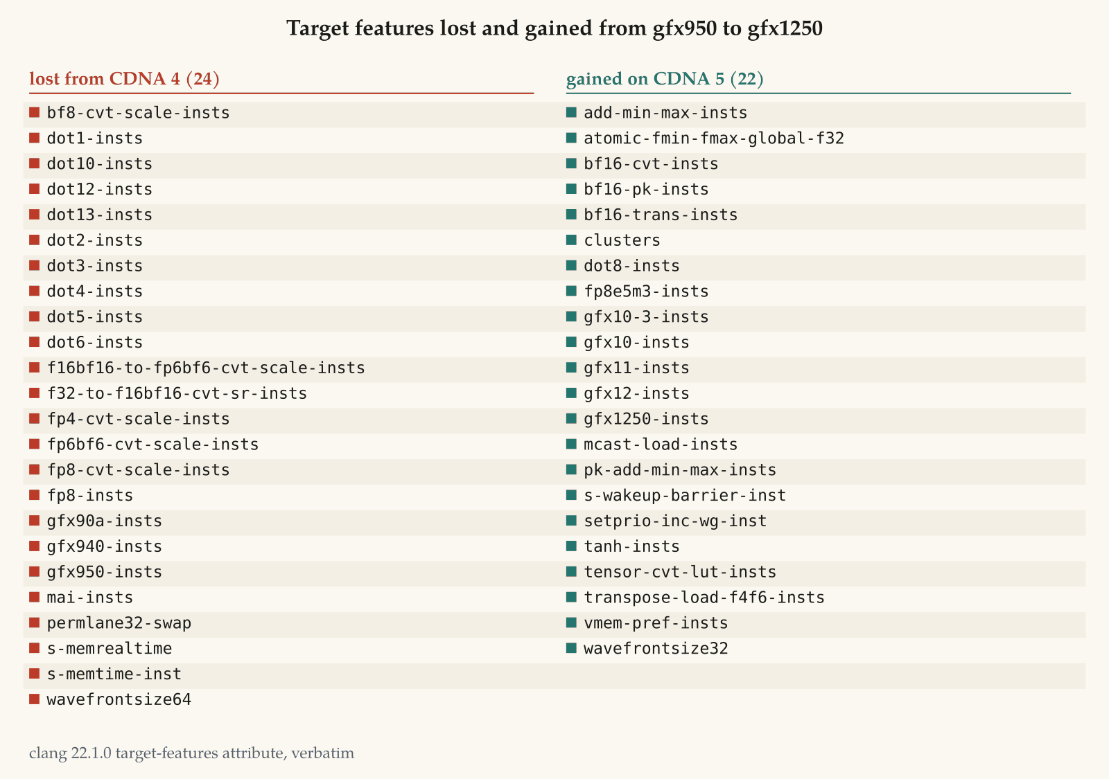
Twenty four features present on gfx950 are absent on gfx1250. Among them: mai-insts, which is the MFMA family; wavefrontsize64, replaced by wavefrontsize32; the entire dot instruction lineage; every one of CDNA 4’s block-scale conversion instructions; and s_memtime and s_memrealtime, so even reading a clock changes.
Twenty two features are new, and they read like a list of things a CUDA programmer would recognise: clusters, a scheduling group above the workgroup of the kind Hopper introduced; mcast-load-insts, multicast loads; vmem-pref-insts, explicit prefetch; tensor-cvt-lut-insts; transpose-load-f4f6-insts; and fp8e5m3-insts.
What replaces it, and what does not change
Counting what disappeared is the easy half. The more useful question is what CDNA 5 puts in its place, and the compiler answers that too.
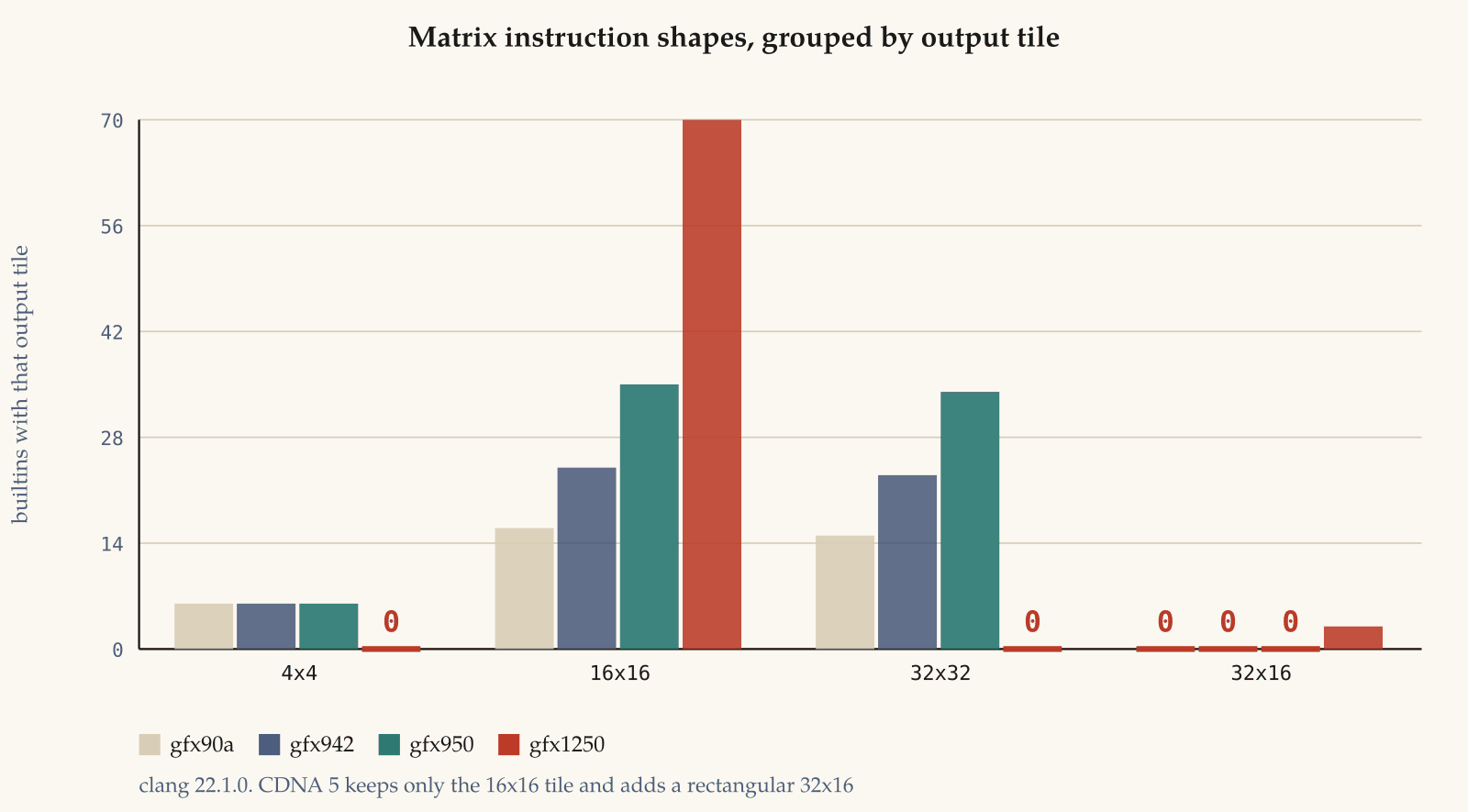
Group the matrix builtins by the shape of the tile they produce. Every AMD datacenter target from gfx90a to gfx950 offers three output tiles: 4x4, 16x16 and 32x32. On gfx1250 the 4x4 and 32x32 families are gone entirely.
What survives is 16x16, plus one new rectangular 32x16, and the K dimension deepens: the largest K on a 16x16 tile goes from 64 on gfx942 to 128 on gfx950 and stays at 128 on gfx1250, now on both surviving tiles.
That is a narrower and deeper instruction set. Eighteen distinct shapes on gfx950 become six on gfx1250.
Fewer tile choices means less for a tuner to search over, which is a small mercy given that the tuner has to start from nothing, and a deeper K means more operand reuse per instruction, which is the direction every matrix unit has been moving on both sides of the market.
Then the question I actually wanted answered. This whole piece has argued that AMD’s distinguishing choice is paying area for registers, and that this is why it never needed a tensor memory.
Does that survive an ISA fork?
So I ran the accumulator sweep again on gfx1250, with a WMMA kernel instead of an MFMA one, and pushed until the allocator gave up.
It gives up at 1,024 registers per lane. A gfx1250 lane has twice the architectural registers of a gfx942 lane, and half as many lanes per wave.
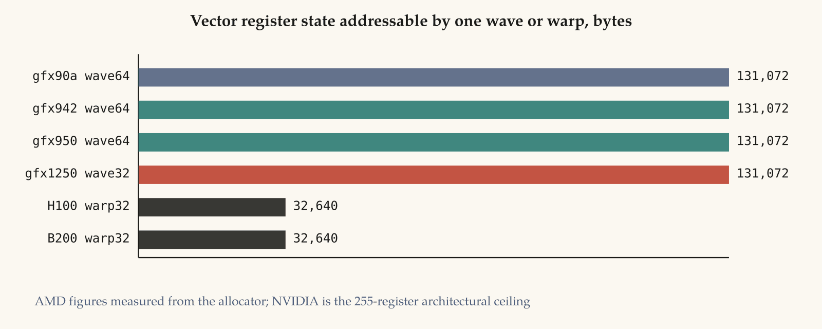
512 registers times 64 lanes is 32,768 words. 1,024 times 32 is 32,768 words. A wave on CDNA 3 and a wave on CDNA 5 address exactly the same 128 kilobytes of vector register state.
AMD threw away the entire matrix instruction set, changed the wave width, moved to a workgroup processor, adopted clusters and multicast loads, and did not move the register budget by one byte.
I did not expect that, and I think it is the most informative single fact in the whole census. The fork is an encoding fork. The architectural philosophy underneath it, spend transistors on register file and let the kernel keep its working set in registers, is intact.
Whatever else changes, an AMD wave will still be able to hold an accumulator that an NVIDIA warp cannot, by roughly four times, and AMD will still not need a separate address space to put it in.
One last thing the compiler gives away. The hazard contract survives as an idea and not one instruction of it survives as text:
gfx942   s_waitcnt lgkmcnt(0)   s_nop 4
gfx950   s_waitcnt lgkmcnt(0)   s_nop 5
gfx1250  s_wait_kmcnt 0x0   s_wait_xcnt 0x0   s_delay_alu instid0(VALU_DEP_1)
The unified GCN counters split into separate ones per traffic class, a counter that did not exist before appears, and the structural no-op is replaced by an explicit ALU dependency delay.
Same principle, every mnemonic renamed, the counters re-partitioned. Anyone who has memorised the waiting rules for CDNA has to memorise them again.
I want to be careful about credit here, because the qualitative version of this observation is not mine. Chips and Cheese read the gfx1250 patches in LLVM in July and described the workgroup processor structure and the matrix unit shapes.
SemiAnalysis, in its Advancing AI coverage three weeks ago, stated plainly that MI455X uses a completely different ISA from MI355X, that every kernel must be independently rewritten and tuned, and characterised gfx1250’s ISA as close to Hopper’s. Both were there before me.
What I have added is the number, the method that produces it in about four seconds on a laptop, and the family-level decomposition that shows the two matrix instruction sets are strictly disjoint rather than overlapping.
And one corroboration worth flagging. SemiAnalysis reported that gfx1250’s matrix engine speaks NVFP4 natively, citing a scale-format enum that includes an e5m3 member and a gfx1250-compiled NVFP4 GEMM already shipping inside AITER.
My feature census independently shows fp8e5m3-insts present on gfx1250 and absent from every CDNA target before it. Two different artefacts, same conclusion.
Now the interpretation, and this is where I think the obvious reading is wrong.
The obvious reading is that AMD has thrown away its software investment, and against the census that reading has force: 16,177 tuned assembly kernels and 2.9 million shape mappings are worth nothing on a target that cannot encode the instructions they are built from. AITER’s fastest paths are hand-written wave64 assembly. Every one is a rewrite.
But look at what the corpus is. Not knowledge, a lookup table. The knowledge sits in the generator, in the parameter space, in knowing which of those 57 dimensions matter and how they interact, and in the harness that runs the search.
Tensile is a program that emits kernels, and retargeting a generator is work but not the same work as rediscovering what to generate. What has to run again is the campaign, on hardware AMD must own, for every part and every harvest bin. That is expensive in machine time and calendar time rather than in insight.
Which is precisely what AMD’s July announcements are about, and it took me a while to see them as a coherent response rather than as agent marketing.
ROCm.ai bundles a CLI, a set of AMD-authored skills for coding agents, and Hyperloom, an open-source agentic system whose stated job is automating end-to-end inference workload optimisation.
Read against the census, that is not a developer-relations play. It is an attempt to industrialise the search, because the search is the cost, and because a company that has just invalidated its own tuning corpus and has fewer internal cluster hours than its competitor needs the search to get cheaper by more than the corpus got smaller.
Whether it works is empirical, and the evidence so far cuts both ways.
On the encouraging side, AMD’s GEAK v4 write-up reports serving throughput gains on real workloads rather than on kernel microbenchmarks: 60 percent on Qwen3.5-27B-FP8, 96 percent on Qwen3-14B-FP8, 42 percent on Minimax-M3-MXFP8.
Those are AMD’s own numbers on AMD’s own hardware, so discount accordingly, but they are end-to-end serving throughput on named models, which is the hard version of the claim and not the easy one.
Against that, KernelBench-Verified showed that when the baseline is TF32 and the tests are hidden, the best model produces a geometric mean of 0.88 times rather than the 1.43 the earlier literature reported, which suggests much of the reported gain was the distance between PyTorch’s defaults and PyTorch’s available settings.
My reconciliation last year was that the value sits in the harness rather than the model: the profiler, the knowledge base, the end-to-end gate. GEAK v4’s own description of itself is now unusually direct evidence for that.
It puts control flow, budget loops, fan-out, verification and stop conditions in deterministic JavaScript, and invokes the model only for structured technical judgment.
That is a harness with a model bolted into it at the points where judgment is needed, which is exactly the shape the KernelBench correction implies you need.
Where I might be wrong
The matrix builtin count is a count of compiler builtins, not of encodable instructions. Clang exposes builtins for the instructions LLVM has intrinsics for, and it is possible that gfx1250 encodes something MFMA-shaped that has no builtin and that AMD reaches through inline assembly.
I looked for a fallback and did not find one, and the feature bit mai-insts being absent is a stronger signal than a missing builtin, but absence of a builtin is not proof of absence of an encoding.
I have not run a single instruction on AMD hardware. Everything here is compiler behaviour, published specification, repository content and arithmetic.
Compiler behaviour is a good proxy for what is encodable and a poor proxy for what is fast. Where I quote performance numbers they are somebody else’s, and I have tried to say whose.
The Tensile census is a snapshot of one branch of one repository, and that branch is called develop_deprecated with a head commit from June 2025.
The gfx942 numbers in particular are almost certainly not the current state, and the gfx950 tuning did not exist in the tree I cloned.
I believe the shape of the result, that the tuning surface is millions of measured decisions over a space of about ten to the twenty second, is robust to the snapshot. The specific integers are not.
The 120 bit parameter space is an upper bound computed by summing the log of observed cardinalities, and it assumes an independence that certainly does not hold: many combinations are invalid, and Tensile’s protocol exists precisely to avoid enumerating them.
Read it as the volume the search has to reason about, not the number of legal kernels. It also treats the macro tile as one parameter with 249 observed values rather than three separate dimensions, which makes it conservative in the other direction.
The bytes-of-state-per-FLOP ratio is a derived quantity with a choice baked in, namely that scratchpad and register file are commensurable. They are not, exactly.
LDS is shared across a workgroup and registers are private to a lane, and 228 KB of Hopper shared memory is not interchangeable with 228 KB of register file.
The ratio is a way of seeing a trend across generations, and I would not defend a comparison between two parts that differed by ten percent on it. Finally, the reading that AMD’s corpus is a lookup table and the knowledge is in the generator is an argument, not a measurement.
Somebody with a Tensile retargeting on their hands could tell me it took eighteen months, and I would have no basis to argue.
Five predictions, dated
I score these publicly, so here they are with a resolution date and a criterion.
By the end of 2027, hipBLASLt or its successor will ship a gfx1250 logic tree whose count of tuned problem shapes is at least a quarter of the gfx942 tree’s at the same point in that part’s life. If the retarget is as cheap as I argue, this is easy. If it is not, this is where it shows.
By the end of 2027, AMD will not ship a compatibility layer that lets an MFMA-based kernel run unmodified on gfx1250. Emulation is possible and would be slow enough to be pointless, and I do not think they will bother.
By mid 2027, a published Hyperloom or GEAK result will report an end-to-end inference gain above 15 percent on gfx1250 with no human kernel author in the loop, on a model somebody else chose. The same claim on gfx950 is already met on AMD’s own numbers; the question is whether it transfers to a target with no tuning corpus behind it, which is the load-bearing question for the whole strategy.
By the end of 2027, at least one serious third-party project will publish a kernel for gfx1250 that beats AMD’s own library on a shape that matters, and will do it in Gluon or Triton rather than assembly. The open ISA has never produced a competitive third-party GEMM. If it is going to, the moment when the vendor’s own corpus is empty is the moment.
By the end of 2028, NVIDIA will not have moved hazard management out of the instruction control field and into architectural instructions. The choice is an area and energy decision from 2012 and there is no sign of a reversal.
And the one I got wrong last time. In July 2025 I predicted at least one more CUDA-compatibility project would lose its funding. Qualcomm announced an all-stock acquisition of Modular on 24 June 2026, valued near 3.9 billion dollars, and closed it on 29 July. That is not losing your funding.
What the whole thing adds up to
I came into this expecting to write that AMD’s openness is undervalued, and I am leaving with a more specific and less comfortable version of that.
The openness is real and deeper than the marketing suggests. The dispatch packet is a documented struct. The code object is an ELF file standard tools read. The target feature axes are orthogonal with a neutral value, which is better engineering than the alternative.
The hazard model is expressible in the instruction stream, so hand-written assembly is a viable production strategy and third parties can pursue it. The compiler is upstream. That I could do all of the work in this piece on a machine with no GPU in it is a direct demonstration of the value.
Openness makes that cost visible rather than smaller. That is still the more useful of the two situations, because a measurable cost is one somebody can attack with automation.
Then AMD did the one thing that makes the cost bigger, which is change ISA families between generations, at the moment it is shipping into gigawatt-scale commitments. Zero of seventy five. I do not think that was a mistake, exactly.
Converging the datacenter and consumer instruction sets is the right long-run move for a company that cannot afford two of everything, and gaining clusters, multicast loads, prefetch and a native NVFP4 path is worth something real.
But it means the next eighteen months of AMD’s software story is a rerun of the tuning campaign, with agents in the loop instead of engineers, on fewer machines than the competitor has.
It is a real bet, it is falsifiable on a timescale of months, and we will know.
Confidence dossier
Every load-bearing claim in this piece, properly graded manually.
M gfx950 to gfx1250 carries over 0 of 75 matrix builtins; gfx90a to gfx942 and gfx942 to gfx950 carry 100 percentm1_isa_census.py, clang 22.1.0
M clang rejects __builtin_amdgcn_mfma_f32_32x32x8f16 on gfx1250 and gfx1251 with ‘needs target feature mai-insts’m1_isa_census.py.
M gfx1250 loses 24 gfx950 features including mai-insts, wavefrontsize64, all dot-insts, all CDNA4 scale conversions, s_memtime, s_memrealtimem1_isa_census.py
M gfx1250 gains 22 features including clusters, mcast-load-insts, vmem-pref-insts, tensor-cvt-lut-insts, transpose-load-f4f6-insts, fp8e5m3-insts, wavefrontsize32m1_isa_census.py
M AMDGPU builtins in clang: 443 at LLVM 20.1.2, 788 at LLVM 22.1.0, 345 added, 0 removedm1_isa_census.py.
M Builtins available per target: 244 gfx90a, 274 gfx942, 362 gfx950, 477 gfx1250m1_isa_census.py.
M MFMA builtins per target: 31 / 39 / 47 / 0. SMFMAC: 6 / 14 / 28 / 0. WMMA: 0 / 0 / 0 / 73m1_isa_census.py
M Target feature counts: gfx90a 27, gfx942 34, gfx950 48, gfx1250 46, gfx1251 46m1_isa_census.py.
M gfx942 has xf32-insts; gfx950 does not. gfx950 adds 15 features over gfx942clang 20.1.2 feature diff.
M A gfx942 lane holds 24 independent 32x32x8 MFMA accumulators (384 registers) with zero spill and the whole 512-entry file allocated; 25 is where scratch traffic startsm5_cdna5.py, full sweep.
M The gfx942 spill tail is not monotone: 25 to 29 spill, 30 does not (500 registers, 480 of accumulator), 31 and 32 spill againm5_cdna5.py, every N from 1 to 34.
M A gfx1250 lane holds 1,024 architectural registers in wave32; the allocator caps vgpr_count at 1024 and first spills at 128 WMMA accumulatorsm5_cdna5.py plus a manual probe to N=256.
M 512 registers x 64 lanes and 1,024 x 32 lanes are both 32,768 words, so a CDNA 3 wave and a CDNA 5 wave address the same 128 KB of vector register statearithmetic on the two measured ceilings.
M Output tiles per target: gfx90a, gfx942 and gfx950 all offer 4x4, 16x16 and 32x32; gfx1250 offers 16x16 and a new 32x16 onlym5_cdna5.py.
M Distinct matrix shapes fall from 18 on gfx950 to 6 on gfx1250; largest K on a 16x16 tile is 64 on gfx942 and 128 on gfx950 and gfx1250m5_cdna5.py.
M The hazard instructions are all renamed on gfx1250: s_waitcnt lgkmcnt and s_nop become s_wait_kmcnt, s_wait_xcnt and s_delay_alum5_cdna5.py.
M Back-computed FLOPs per clock per unit land within 0.7 percent of a power of two on every AMD part and 4 to 6 percent off on H100 and B200, so at least one published NVIDIA input is not the number usedm4_model.py.
M At 16 accumulators the allocator reports 288 registers of which 32 AGPR, and sets ACCUM_OFFSET to 256m2_hazards_registers.py
M gfx90a, gfx942 and gfx950 emit .amdhsa_accum_offset and .agpr_count; gfx1250 emits neither and defaults to wave32m2_hazards_registers.py.
M A gfx942 code object for a single MFMA loop is 4,848 bytes: ELF64, OS/ABI AMDGPU_HSA, 15 sections, 13 symbolsllvm-readobj on ko_gfx942.hsaco.
M e_flags 0x54C decodes to EF_AMDGPU_MACH_AMDGCN_GFX942 plus XNACK_ANY_V4 plus SRAMECC_ANY_V4llvm-readobj --file-headers.
M The kernel descriptor is 64 bytes in .rodata; decoded rsrc1 0x00af0082, rsrc2 0x00000084, rsrc3 0x00000000, properties 0x0008kernel descriptor decode.
M Same source, 1,472 bytes of .text on all three CDNA targets; 113 bytes differ gfx90a to gfx942, 33 bytes gfx942 to gfx950llvm-objcopy byte diff.
M hipBLASLt logic tree: 145 files, 26,248 solutions, 16,177 distinct kernel names, 2,905,048 shape mappings, 310 MBm3 census, develop_deprecated at 3a609b0.
M MI200 tuning is split by compute unit count into 104CU and 110CU directories with separate tablesrepository layout.
M The 1,439 distinct gfx942 kernel names encode 56 tuning parameters with more than one observed value, summing to 119.9 bits, which is 1.28e36m6_tuning_space.py.
M The shipped set is 1,439 kernels, 10.5 bits, which is 1.1e-33 of the spacem6_tuning_space.py.
M Bits by group: scheduling and hints 38.7 over 24 parameters, split along K 18.6 over 9, tile geometry 17.8 over 5, vector widths 17.6 over 9, LDS layout 15.4 over 6, XCD mapping 11.9 over 3m6_tuning_space.py.
M Macro tile MT takes 249 distinct values (7.96 bits); WGM 32; GSU 30; WGMXCCG 20; LBSPPA 16; MIWT 14m6_tuning_space.py.
M B* is identical across FP16, FP8 and FP4 to within 1 percent on every part measuredm4_model.py.
M B*: MI300X 246.6, MI325X 217.8, MI350X 287.5, MI355X 312.5, H100 295.4, H200 206.1, B200 281.2m4_model.py.
M Bytes of on-chip state per FP8 FLOP per clock per unit: MI300X 144.0, MI355X 84.6, H100 58.0, B200 32.0m4_model.py.
M Vector register file per chip: MI300X 152 MB, MI355X 128 MB, H100 33 MB, B200 37 MBm4_model.py.
M 70B FP8 with GQA-8 at 90 percent capacity: H100 12,207 KV tokens, MI300X 627,441, MI355X 1,154,785m4_model.py.
M Matrix throughput per clock per unit: MI300X 4,096 FP8, MI355X 8,138, H100 8,543, B200 15,473m4_model.py.
M hipBLASLt has 180 remote branches; its default branch is named develop_deprecated with head from 2025-06-20git ls-remote.
A MI455X: 432 GB HBM4, up to 23.3 TB/s, 40 PFLOPS FP4, 20 PFLOPS FP8, 8 XCDs, CDNA 5; the 19.6 TB/s figure that circulated before launch is supersededAMD MI400 series product page.
M B* for MI455X is 429 at both FP8 and FP4, up 37 percent on MI355X, so the memory-bound regime is shrinkingm4_model.py with AMD published figures.
M MI455X holds 1,945,801 tokens of FP8 KV beside a 70B FP8 model at 90 percent of capacitym4_model.py.
A Helios delivers up to 1.4 exaFLOPS FP8 and 2.9 exaFLOPS FP4 with 31 TB of HBM4AMD MI400 series product page.
A MI355X: 256 CU, 288 GB HBM3E, 8.0 TB/s, 160 KB LDS per CU, 2.5 PF FP16 dense, 10 PF FP4, 1,400 WAMD product page and ROCm workload optimization guide.
A MI300X: 304 CU, 192 GB HBM3, 5.3 TB/s, 64 KB LDS per CU, 4 IODs, 8 XCDs, 256 MB Infinity CacheROCm workload optimization guide.
A CDNA 3 uses FP8 FNUZ variants; CDNA 4 uses OCP variants. TF32 moves to software emulation via BF16 on CDNA 4ROCm workload optimization guide.
A FP64 matrix halves on CDNA 4, 128 versus 256 FLOPs per clock per CUROCm workload optimization guide.
A E4M3FN and E4M3FNUZ share a bit layout, differ in exponent bias by one, so a misread byte is off by a factor of twoAMD Matrix Core blog; Fergus Finn.
A buffer_load_to_lds saves about 100 VGPR per wave and moved a reference gfx950 GEMM from 697 to 1113 TFLOPSROCm workload optimization guide, Gluon section.
A XCD-aware workgroup remapping cut L2 misses from about 5M to 3.1M and added about 67 TFLOPSROCm workload optimization guide.
A XCD clocks vary 3 to 10 percent on one package; XCD0 typically fastest, XCD7 slowest on MI300XROCm workload optimization guide.
A A GEMM stride that is a multiple of 512 bytes causes channel hotspotting on MI300; pad to K+128 when K%256==0ROCm workload optimization guide.
A MI16x16 outperforms MI32x32 on MI300X for GEMM, attributed to power efficiencyROCm workload optimization guide.
A ROCm serialises kernel launches across GPUs from one process; RCCL wants one process per GPU; GPU_MAX_HW_QUEUES=2 recommendedROCm workload optimization guide.
A ROCm 7.0 to 7.8 is the production stream, 7.9 and later is technology preview; production is 7.2.x, preview reached 7.14ROCm release version pages.
A Helios: 72 MI455X, 18 EPYC Venice, up to 2.9 EF FP4, 31 TB pooled HBM4, MI455X at 432 GBAMD Advancing AI 2026 materials.
A AMD claims Helios delivers up to 30 percent more tokens per dollar than the leading competitive solutionAMD press release, 23 July 2026.
A ROCm.ai comprises ROCm CLI, AMD Skills for coding agents, and Hyperloom, an open-source agentic optimisation systemAMD newsroom, 23 July 2026.
B vLLM issue 45562 and PR 45720: FNUZ KV bytes read as FN on gfx942 degraded GSM8K accuracy; the dtype fix recovered itvLLM GitHub, June 2026.
B AITER issue 3807: building for gfx942 and gfx950 together returned the OCP dtype on an MI300XROCm/aiter GitHub, June 2026.
B Both AITER MLA backends share the assembly decode kernel mla_decode_fwd; most of the 1.2 to 1.6x gain is attributed to itvLLM blog, 27 February 2026.
B MI300X SGLang throughput roughly doubled between December 2025 and January 2026, attributed to AITERSemiAnalysis InferenceX v2, via HyperAccel analysis.
B MI455X is gfx1250 and MI430X is gfx1251; gfx1250 is WGP-based, wave32, and listed as an APU in LLVMChips and Cheese, July 2026.
B gfx1250’s matrix engine supports NVFP4 natively; a gfx1250 NVFP4 GEMM code object already ships in AITERSemiAnalysis, Advancing AI 2026 coverage.
B SemiAnalysis states every MI355X kernel must be independently rewritten and tuned for MI455XSemiAnalysis, Advancing AI 2026 coverage.
B GEAK v4 reports serving throughput gains of 60 percent on Qwen3.5-27B-FP8, 96 percent on Qwen3-14B-FP8 and 42.2 percent on Minimax-M3-MXFP8, self-measuredAMD GEAK v4 technical article, 23 July 2026.
A GEAK v4 puts control flow, budget loops, fan-out, verification and stop conditions in deterministic JavaScript and invokes the model only for structured technical judgmentAMD GEAK v4 technical article.
A Hyperloom orchestrates five components: TraceLens for bottleneck identification, GEAK and Arbor for optimisation in parallel, over Magpie and IntelliKit for profilingROCm Hyperloom documentation and repository.
B KernelBench-Verified: best model reaches 0.88x geomean against a TF32 baseline with hidden testsarXiv:2607.16241.
C The CDNA corpus is a lookup table and the reusable asset is the generator plus the search harness, so retargeting costs machine time rather than insightauthor’s argument.
C ROCm.ai and Hyperloom are best read as an attempt to industrialise the tuning search in response to the gfx1250 retargetauthor’s inference from timing and content.
C The absence of an MFMA fallback encoding on gfx1250 is inferred from the absent mai-insts feature bit, not provedauthor’s inference.
B InferenceX, 20 May 2026: MI355X SGLang FP8 up to about 40 percent cheaper per million tokens than B200 on GLM-5 8K/1K, peak gap at 18 tok/s/user, 22 cents against 30; B200 ahead above about 90 tok/s/userInferenceX blog post, measured 2026-05-20.
B InferenceX overview, July 2026 TCO model: MI355X 35.5 cents per million on 8K/1K FP4 against B200 at 30.4, i.e. 17 percent more expensive; the long-context agentic scenario lists a far larger gapInferenceX overview page.
B The reversal is attributed to B200’s NVFP4 path shipping and to AMD lacking a disaggregation or wide expert parallel recipe for that modelInferenceX blog post, same source.
A Qualcomm acquired Modular in an all-stock deal valued near 3.9 billion dollars, announced 24 June 2026, closed 29 July 2026Qualcomm and Modular announcements, SEC filing.
C A memory-bound decode bounds the kernel gap above by the ratio of achieved HBM bandwidths, which is why an immature kernel layer costs less in that regimeauthor’s argument.
C The inference and training asymmetry follows from hot-kernel-set size, the memory-bound regime and capacity, not primarily from software maturityauthor’s argument.
C A figure of about 92 percent CUDA device API coverage for HIP circulates in channel material and could not be traced to a primary AMD sourceauthor’s search.
A The kernel descriptor for the sample kernel sets ACCUM_OFFSET to 0, so AGPRs begin at register 4, and the metadata agrees: 20 registers total of which 16 are AGPRskernel descriptor decode, cross-checked against .agpr_count.
A vmcnt returns in order and lgkmcnt does not, which is why nonzero lgkmcnt waits are rare when scalar loads are involvedLLVM AMDGPUUsage and generated code.
A Unpadded shared layouts cause 2-way to 4-way LDS bank conflicts, cutting the effective rate from 256 B/cycle to 64-128ROCm workload optimization guide, Gluon section.
A Eight MI300X modules are fully connected by seven Infinity Fabric links each; AMD advises using one GPU or all eight for collectivesROCm workload optimization guide.
A rocprof, rocprofv2, ROCProfiler and ROCTracer are deprecated with end of support announced for 2026 Q2; PyTorch still depended on ROCTracer at 7.2.1ROCm 7.2.1 release notes.
D AMD’s long-run direction is a single unified datacenter and consumer ISA, of which gfx1250 is the first datacenter memberspeculation consistent with the feature set.
Tier Definition
M. Measured here. Produced by a script in this piece on a machine with no GPU, reproducible from the appendix.
A. Primary and verifiable. Vendor documentation, specification, or repository content read directly.
B. Credible secondary. Reported by an identified party with a method, not independently reproduced here.
C. Inference. Follows from the evidence but is an argument rather than a measurement.
D. Speculation. Stated as such.
